SiC-Based Half-Bridge Converter: Impact of Gate Resistance on Switching Behavior and Loss Estimation
ABSTRACT
This study explores the behavior of SiC MOSFETs in a half-bridge converter, emphasizing simulation and experimental validation under both ZVS and non-ZVS conditions. Fast switching and high efficiency make SiC attractive, but parasitic-induced oscillations and EMC require careful design. The influence of gate resistance on switching dynamics and loss mechanisms is analyzed, showing that higher gate resistance reduces oscillations but increases switching losses. For estimating the MOSFET dissipated power, traditional current sensing with current probes or shunt resistors introduces parasitic elements that affect the transistor switching and compromise the instantaneous power measurements. As a result, alternative methods were employed for loss estimation in high-frequency SiC converters. Results demonstrate that increasing gate resistance from 3 Ω to 30 Ω reduces oscillation amplitude by 41%, while increasing switching losses by 53.8%. These findings support gate-drive optimization in SiC-based converters.
KEYWORDS
SiC MOSFET; Gate Resistance; Switching Losses
I. INTRODUCTION
Silicon Carbide (SiC) MOSFETs have become increasingly prominent in high-frequency and high-efficiency power conversion applications due to their fast-switching capabilities, low conduction losses and capability to operate at elevated junction temperatures [1]. However, their fast-switching behavior introduces significant challenges regarding switching noise, electromagnetic compatibility (EMC), and accurate loss estimation [2]. One of the key difficulties lies in measuring instantaneous power losses, which traditionally involves capturing the product of drain-to-source voltage and drain current. In practical setups, especially at high frequencies, inserting current sensors such as current probes in the drain path introduces considerable parasitic inductance, distorting the switching waveforms and compromising power measurement accuracy [3]. This effect renders conventional methods unreliable for evaluating power losses in SiC-based converters [4].
Gate resistance adjustment has been employed to mitigate oscillations caused by the interaction between device parasitic elements and printed circuit board (PCB) layout. Increasing the gate resistance reduces voltage and current ringing, and consequently lowering electromagnetic interference (EMI). However, this comes at the cost of higher switching losses, as slower transitions lead to increased overlap between voltage and current during switching [5]. Thermal measurements further confirmed that higher gate resistance values correlate with elevated device temperatures, reinforcing the trade-off between (EMI) mitigation and energy dissipation [6].
Given the limitations of intrusive current measurement techniques and the inherent trade-offs in gate drive tuning, this study uses an alternative method for estimating switching losses in SiC converters [7]. By comparing the measured input and output power, it is possible to derive reliable estimates of energy dissipation without altering the converter’s dynamic behavior [8]. This method is particularly relevant for SiC MOSFETs, whose nanosecond-scale switching transitions make conventional measurements highly susceptible to parasitic circuit elements and probe-induced distortions. The insights presented contribute to developing more accurate evaluation techniques and optimized gate driving strategies for high-performance SiC and GaN power electronics [9] - [13].
Moreover, the selection and configuration of gate resistors directly affect switching speed, transient behavior, and circuit stability. The interaction between parasitic elements, such as inductances and intrinsic MOSFET capacitances, and gate drive parameters can give rise to resonant oscillations, overvoltages, and waveform distortions. These effects pose challenges to both converter design and the accurate experimental characterization of switching behavior. Therefore, a thorough understanding of the interplay among gate resistance, parasitic components, and the measurement setup is essential for achieving reliable and high-efficiency converter operation. Thus, a non-intrusive loss estimation approach for SiC converters is presented and validated in this study.
II. SIMULATION OF SWITCHING BEHAVIOR, LOSSES, AND GATE RESISTANCE EFFECTS IN SIC CONVERTER
The simulation was used to verify the circuit’s operation before implementation and, if necessary, allow for redesign. Additionally, it provides the ability to observe signals that would not be accessible in experimental setups. The detailed parameters are presented in Table 1.
This simulation considers the effects of parasitic inductances in a half-bridge circuit, shown in Fig. 1. The connection of 40 nH inductances corresponds approximately to PCB traces with a length of 3–4 cm.

The SPICE model provided by the SiC MOSFET manufacturer includes non-ideal characteristics of transistors, such as the junction capacitances and connection inductances.
The parasitic inductances were added externally, with 10 nH and 40 nH values. This inductance value can be determined using equation (1), equation provided from Saturn PCB Design. The 20 nH inductance corresponds to the internal value of the SPICE model.
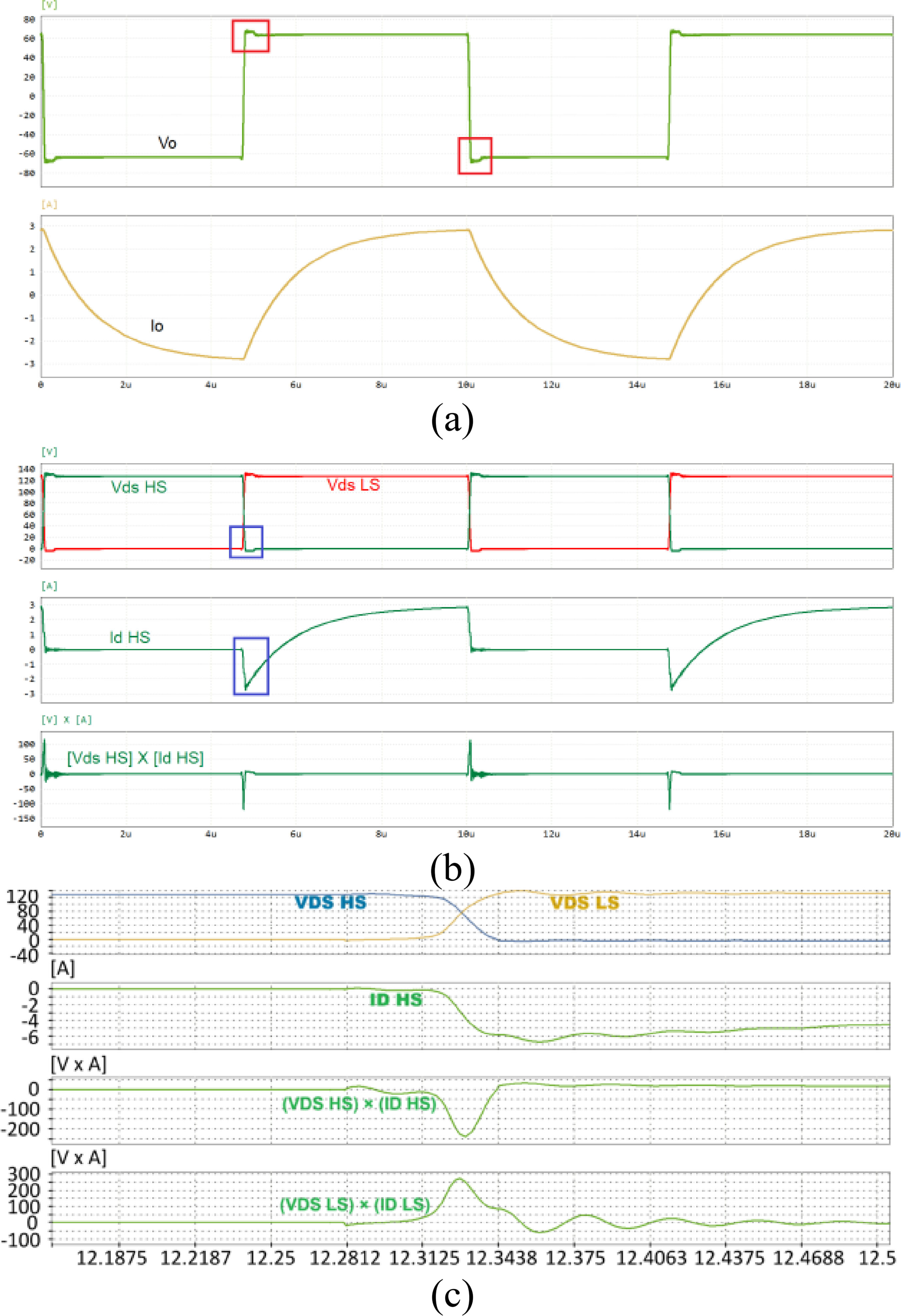
Fig. 2(a) shows the load waveforms. The voltage is a square wave, applied to an RL load. A slight oscillation can be observed during the dead time interval (600 ns), noticeable in the output voltage Vo (marked with the red arrow). During this dead time, conduction occurs through the reverse diode.

Waveforms with soft-commutation.(a) Converter Output Voltage and Current; (b) Vds Signals of the HS and LS Turn-On, Id HS, Instantaneous Power HS and LS; (c) HS and LS Vds signals, HS Drain Current (Id), and HS Instantaneous Power.
Fig. 2(b) illustrates wavesforms of high-side (HS) and low-side (LS) transistors. The rectangle highlights the moment of reverse conduction in the HS MOSFET. Due to the dead time, this reverse conduction initially occurs through the body diode. When the gate signal is applied, as the on-resistance is very low, the current flows through the channel, turning off the diode. This can be seen in the marked area, where a slight decrease in the reverse voltage indicates the transition from diode to channel conduction. These losses during diode conduction are very important, since they occur at the maximum current and the voltage drop is much higher than the channel voltage.
Fig. 2(c) provides a more detailed illustration of the transistor switching behavior during turn-on and turn-off. The instantaneous power, calculated by the multiplication of the current and voltage waveforms, is not dissipated in the MOSFET; instead, this effect occurs during the Vds voltage transitions and the energy exchange between the transistor's capacitances, resulting in a positive peak in one transistor and a negative peak in the other. This characterizes Zero Voltage Switching (ZVS). The switching interval is very short, so the MOSFET's capacitance is enough to provide this soft-commutation. Once the switching transitions are completed, only the conduction loss remains
Despite all the parasitic inductances inserted in the circuit, no relevant oscillations are present in the simulated results, which is a consequence of the soft-commutations at this operation point.
A different topology is used to analyze the switching losses in hard-commutation conditions. Instead of being connected to the DC voltage center tap, the load is moved to the positive terminal, as shown in Fig. 3. The 25% duty cycle, defined for the LS transistor, assures unidirectional load current. Two situations were verified, one with reduced gate resistance (3 Ω) and other with 30 Ω.
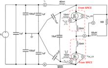
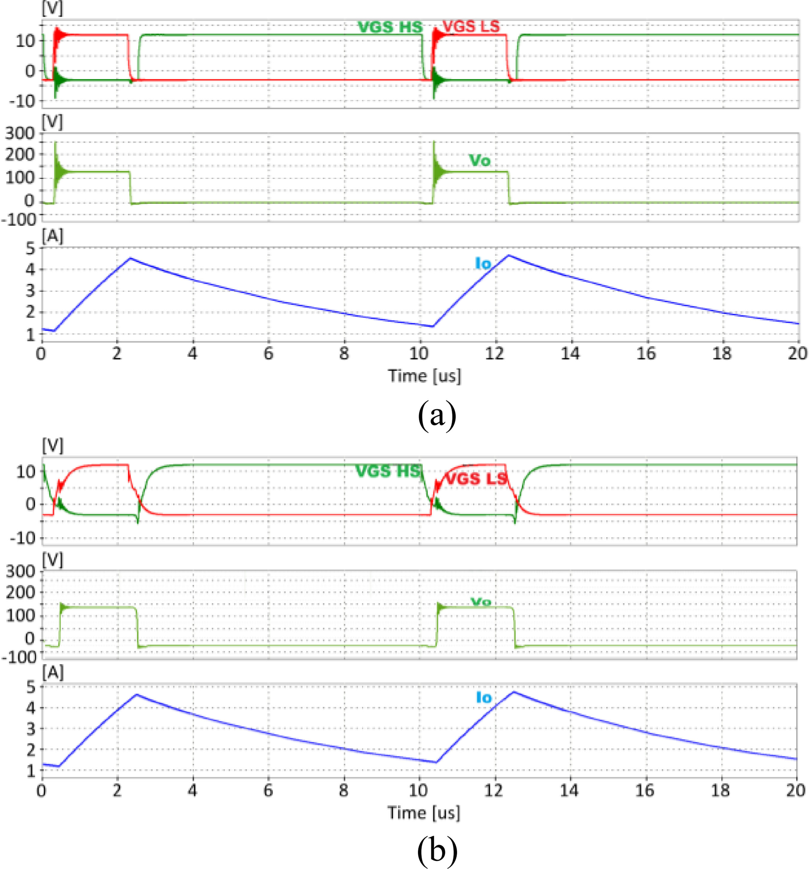
Fig. 4 illustrates the waveforms changing the gate driver resistance, RG, from 3 to 30 Ω. Now the load voltage, Vo, and current, Io, are unidirectional, resulting in a hard-commutation to LS transistor turn-on.
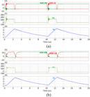
Using RG = 3 Ω (Fig. 4(a)), there is an overvoltage on the load, which reaches 250 V. While the LS transistor is off, the load current flows reversely through the HS MOSFET channel. Due to the dead time, the respective body diode assumes the load current when this transistor is turned off. When the LS MOSFET receives the gate signal, it will take the current, blocking the HS diode. The diode reverse recovery characteristics, especially the junction capacitance, will resonate with the circuit inductances, producing a 24 MHz oscillation. The same load overvoltage is also observed on the HS MOSFET. This oscillation affects the gate-source voltages.
Using RG = 30 Ω, drastically reduces the overvoltage, as shown in Fig. 4(b). Still, the trade-off that occurs paid will be the increase in the commutation power losses, as will be discussed later.
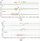
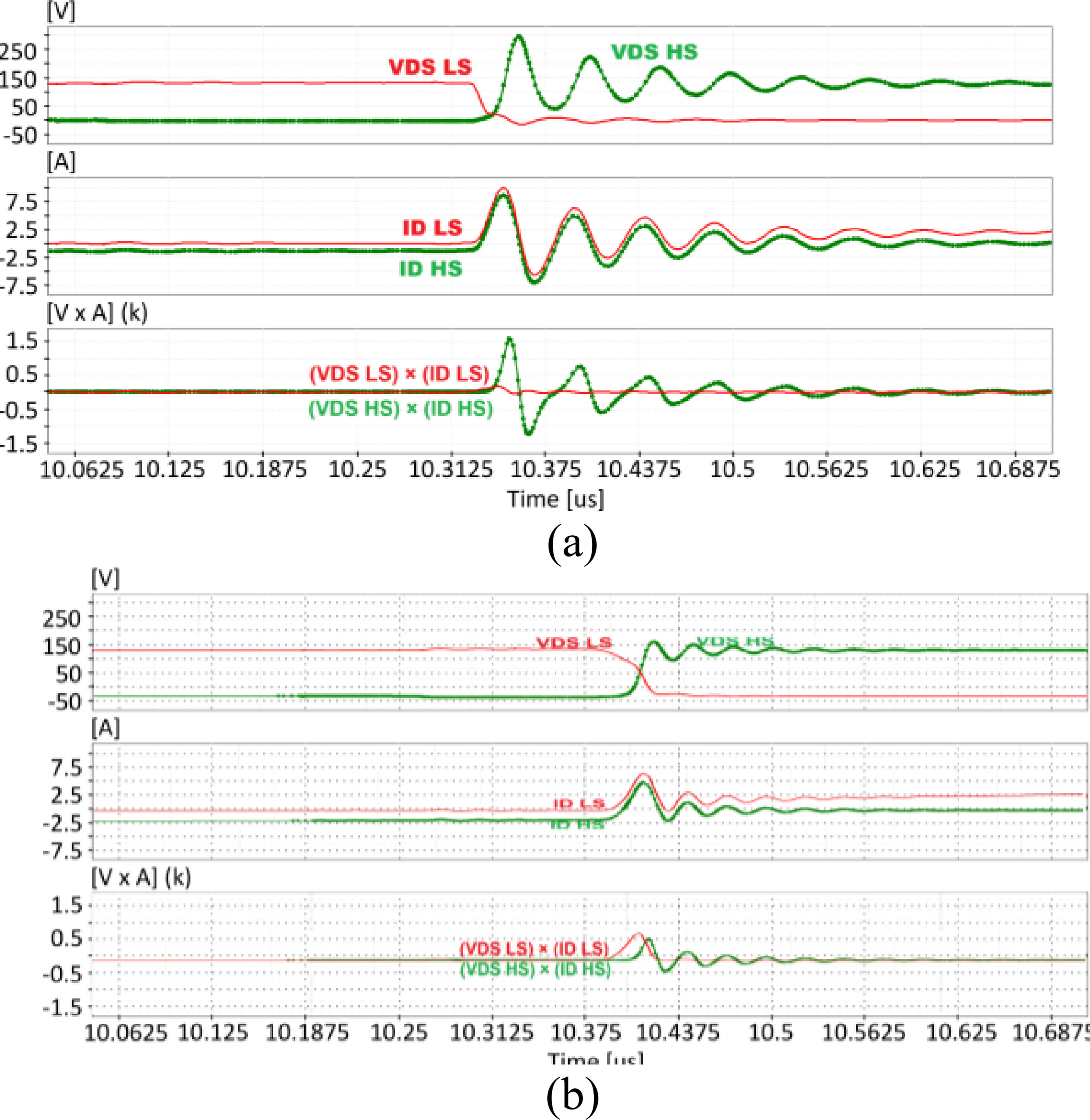
Fig. 5(a) presents the SPICE simulation results illustrating the switching transition details for a gate resistance of RG = 3 Ω, Fig. 5(b) shows the corresponding behavior for RG = 30 Ω. The 24 MHz resonance results in a high overvoltage on the HS switch. It can be observed that increasing the gate resistor reduces the oscillation amplitude and increases the damping rate. There is also a slight increase in the delay between the logic signal and the actual switching of the devices.
Another important result is the changes in the instantaneous power observed on the transistors. In both cases, the oscillatory behavior of the power on the HS MOSFET indicates the dominance of reactive components, which means the expected active power loss is low. However, as the voltage does not oscillate for the LS transistor, the instantaneous power means power losses.
The calculation of the energy dissipated in the transistors is presented in Table 2. The energy was computed using the “INT” function in PSIM, which integrates the instantaneous power over time during the switching transitions of both transistors. For the LS switch, the RG = 30 Ω results in five times more energy dissipation compared to 3 Ω. The HS transistor shows no significant changes. The turn-on of the HS transistor is soft, since there is a ZVS transition when the LS MOSFET turns off and the HS reverse diode assumes the current, regardless of the RG.
Table 2 shows the energy dissipation when the converter operates in ZVS.
The rise time of Vds waveforms for both HS and LS MOSFETs remained nearly unchanged, (see Fig. 6) measuring approximately 14 ns (RG = 3 Ω) and 20 ns (RG = 30 Ω). This limited variation occurs because the Vds transition depends on the load current and the channel characteristics of the MOSFET, rather than on the gate resistance. As a result, the dV/dt remained relatively unaffected by the change in RG.

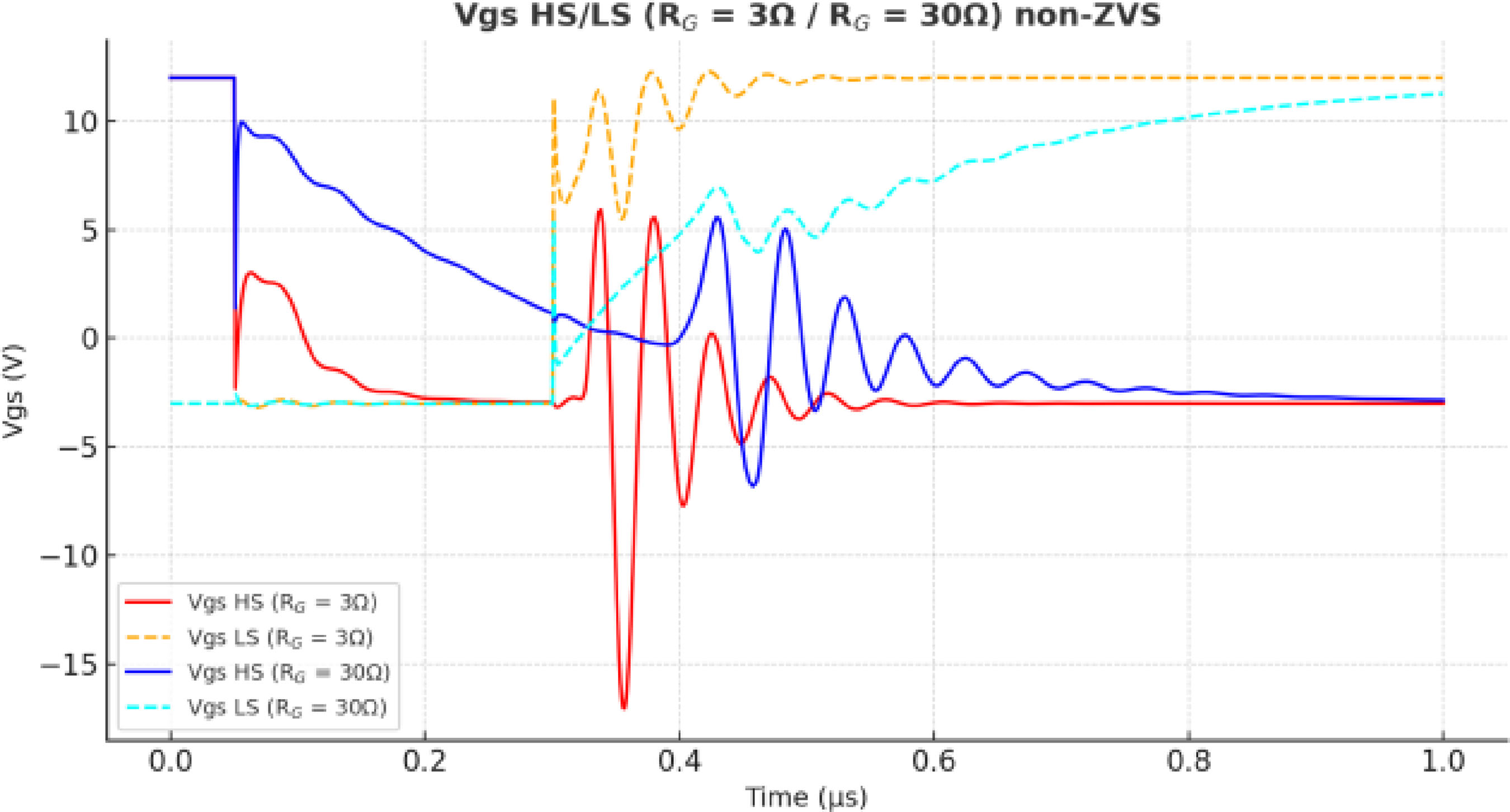
Conversely, the Vgs waveforms exhibited a pronounced dependence on the gate resistance, see Fig. 7. Since the gate circuit can be modeled as an RC network (τ =RG × CG), increasing RG by a factor of ten significantly lengthened the turn-off transient, producing a visible tail in the Vgs HS waveform. This prolonged turn-off delays the full blocking state of the device, slightly shifting the timing of the Vds HS and Vds LS transitions.
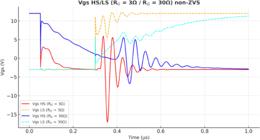
Table 3 shows the energy dissipation when the converter operates in non-ZVS.
III. EXPERIMENTAL RESULTS
The experimental circuit, conceptually, is the same as shown in Fig. 3, operating at 100 kHz with D=25%, defined as an LS transistor. Table 4 shows the SiC MOSFET.
It is important to note that the 1200 V SiC MOSFET used in this study was operated at a comparatively low dc-link voltage due to safety and laboratory equipment constraints. Under these conditions, the device's output capacitance (Coss) becomes a dominant factor in the switching dynamics, accentuating non-ideal transient behavior. These operating conditions, while restricted, still provide valuable insight into the influence of gate resistance and parasitic elements on the device's dynamic performance.
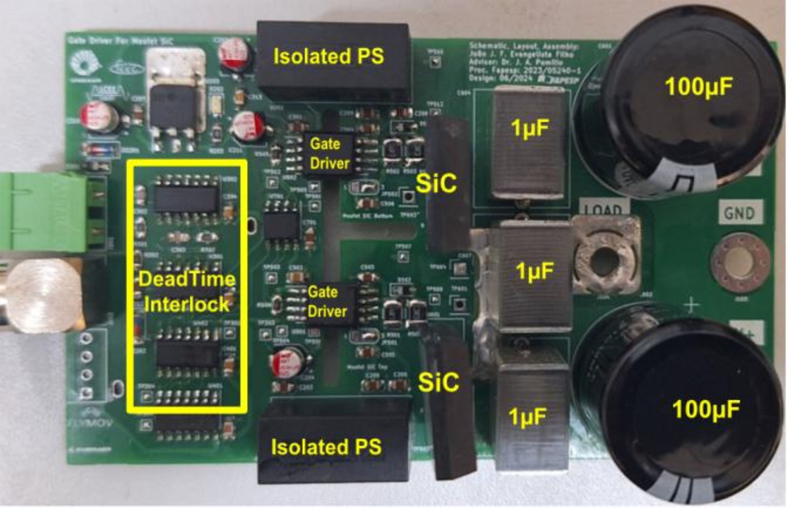
The experiments use the driver and converter board shown in Fig. 8. Integrating the driver and converter into a single board results in a compact layout, reducing the interconnections and minimizing parasitic inductances.

To measure the drain current of the HS and LS MOSFETs using a current probe, a wire was inserted in series with each transistor's drain, as shown in Fig. 9. However, due to the wire length (4 cm), this additional inductance is expected to affect the measured signals. More than this, for connecting the measurement loops, the ceramic capacitors (see Fig. 9) that allow a high-frequency path between the dc source and the transistors are disconnected from the drain, increasing the inductive effect in series with the main path of the switching current. Four test scenarios were conducted, combining the presence or absence of the current loop and the use of gate resistors of 3 Ω and 30 Ω.

SWITCHING TEST WITH CURRENT PROBE, D = 25%, Rg = 3Ω
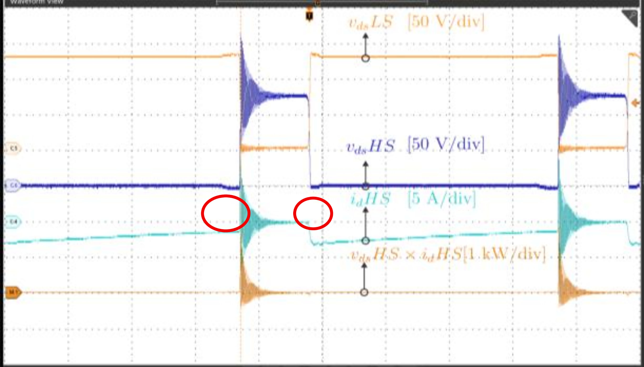
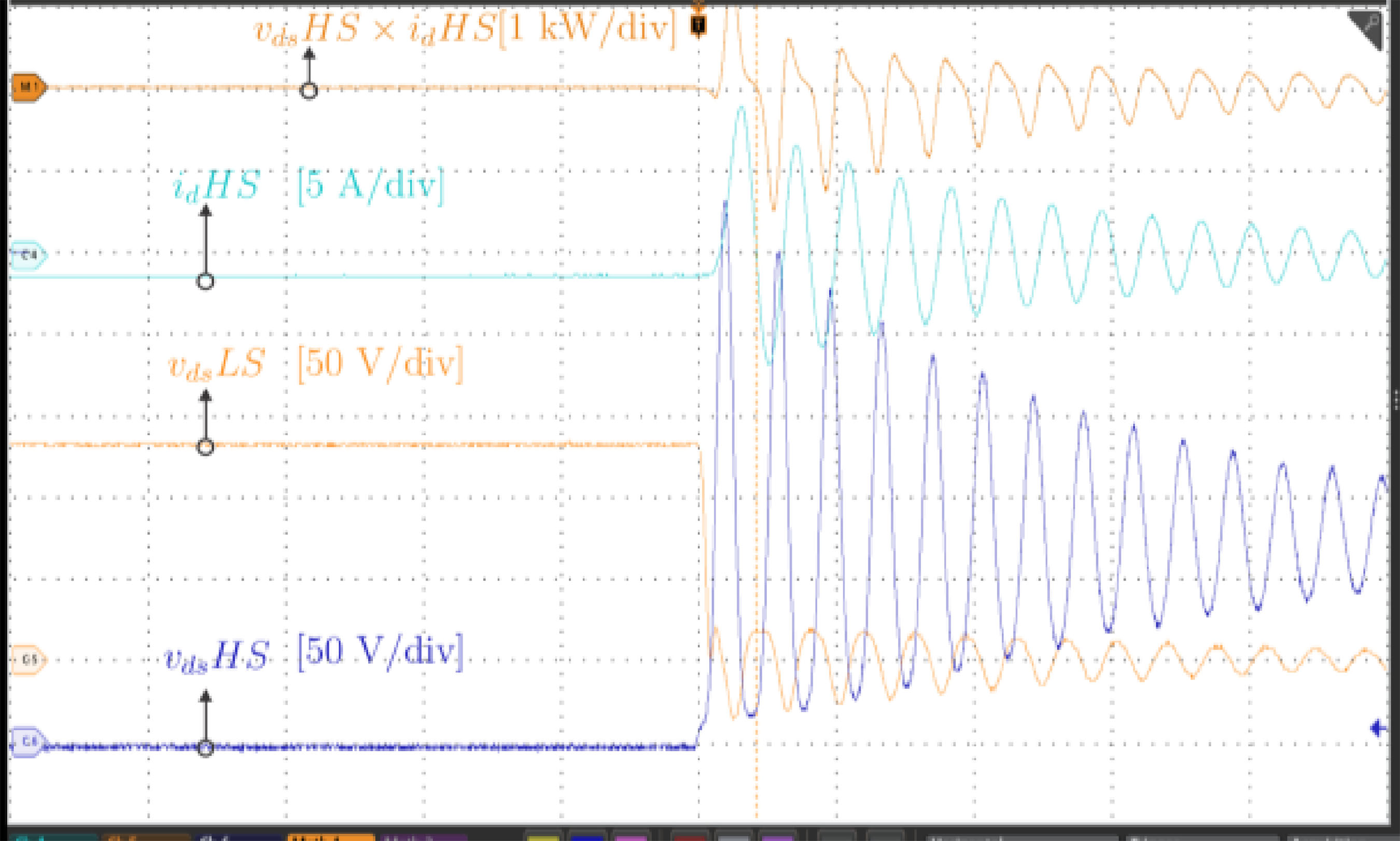
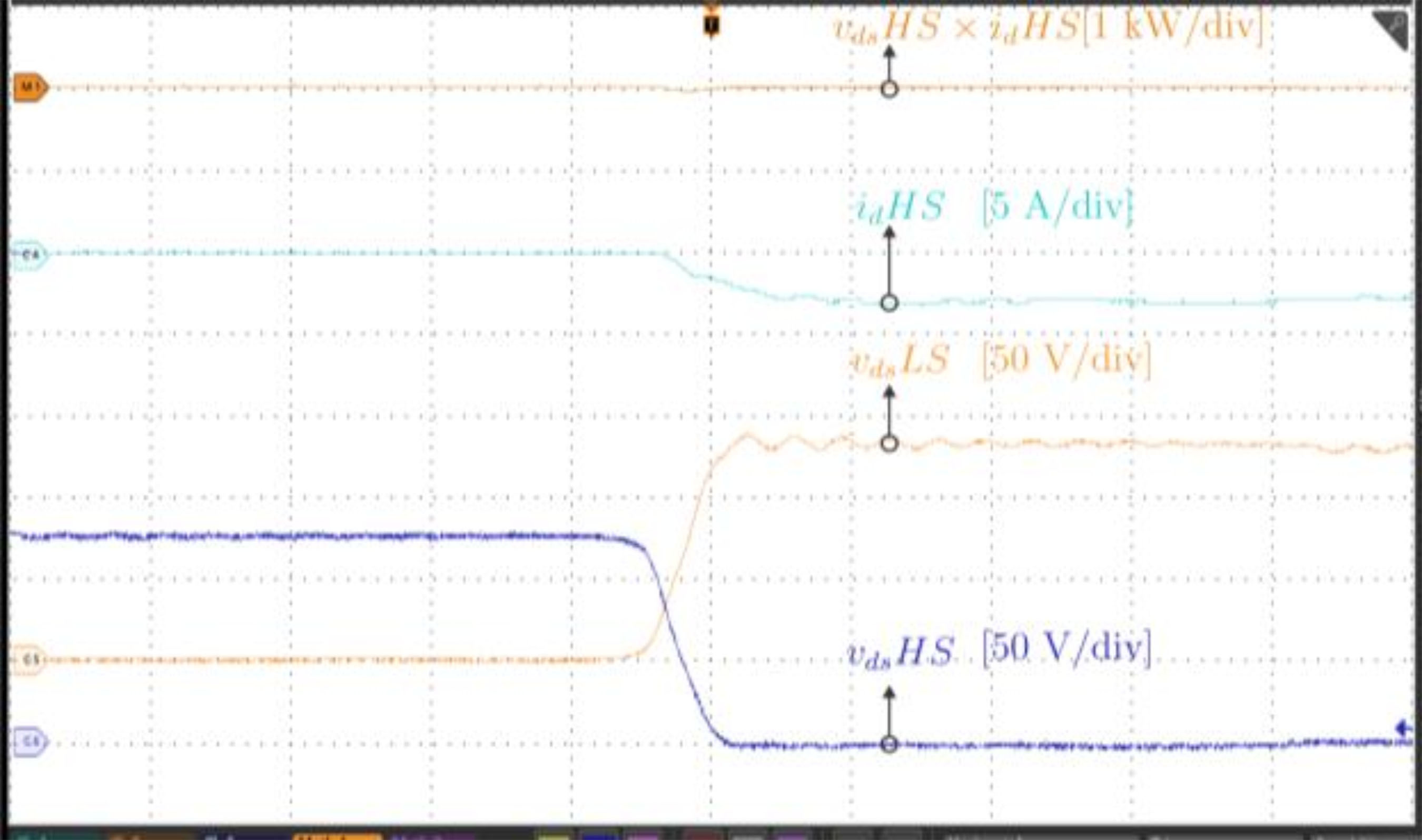
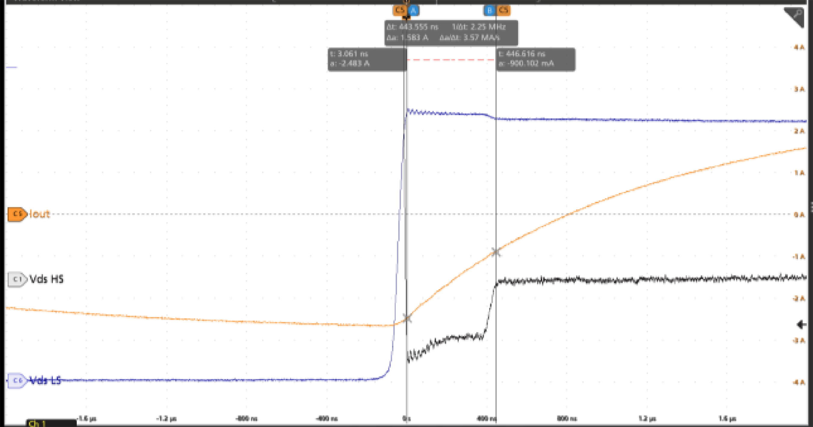
Fig. 10 shows that only the turn-on of the HS MOSFET is noisy. Fig. 11 and 12 highlights the details of this transition. Only the HS MOSFET exhibits significant noise, as it operates in freewheeling mode and undergoes hard-switching, which excites resonances in the circuit. The LS MOSFET, in contrast, shows clean transitions without oscillations. When the LS transistor turns off, due to the dead time, the load current freewheels through the HS MOSFET diode. Due to the devices’ capacitances, the fast commutation behaves like a ZVS, and no resonances or over-voltages are observed in Fig. 12. After the dead time, the gate signal is applied to the HS transistor, and the current is transferred to the channel. When the reverse diode conducts, the Vds HS voltage is more negative than when the current flows through the channel. The HS transistor switches off before the gate signal is applied to the LS transistor and the HS MOSFET reverse diode again assumes the load current. LS transistor turns on, assuming the load current, blocking the diode.
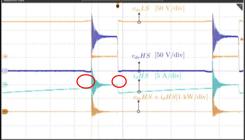
Switching waveforms with current probe and RG = 3 Ω. Vds LS and HS, Id HS, and instantaneous power HS, Horiz: 2 µs/div.

Switching waveforms with current probe and RG = 3 Ω. Vds LS and HS, Id HS, and instantaneous power HS. LS turn-on transition. Horiz: 100 ns/div.
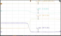
Switching waveforms with current probe and RG = 3 Ω. Vds LS and HS, Id HS, and instantaneous power HS. LS turn-off transition. Horiz: 100 ns/div.
The diode reverse recovery induces a strong oscillation between the HS switch capacitances and the parasitic inductances in the current path. The increase in inductance caused by the placement of the drain current measurement points contributes to the oscillation observed in the HS Vds and in the current. The resonance frequency is around 26 MHz.
The product of (Vds HS × Id HS) does not represent dissipated power but rather energy exchange among the reactive elements in the circuit. The instantaneous power during the turn-off of the HS MOSFET has a near-zero value, confirming the soft-commutation.
The Vgs, see Fig. 13, reflects the HS Vds oscillation, which could lead to multiple switching and simultaneous conduction of both transistors. The observed variation in the Vgs voltage is mainly attributed to the oscillations in the drain current during the switching processes.
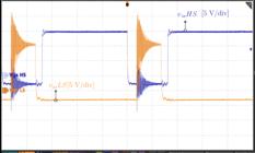
To investigate whether the oscillation originates from a resonance in the gate circuit, consider that, according to the manufacturer's SPICE model, the MOSFET has a gate inductance (Lg) of 12.5 nH and a gate capacitance (Cg) of 4.8 nF. This results in a natural resonance frequency () of approximately 20.5 MHz (2), different from the observed frequency. But since the internal gate resistance is 0.4 Ω and the external one is 3 Ω, the gate circuit is overdamped (3). This means it is not the main cause of the oscillation, but can contribute to increasing the resonance amplitude and duration. These values allow the calculation of a gate resistance of 3.2 Ω required for the RLC gate circuit to be critically damped.
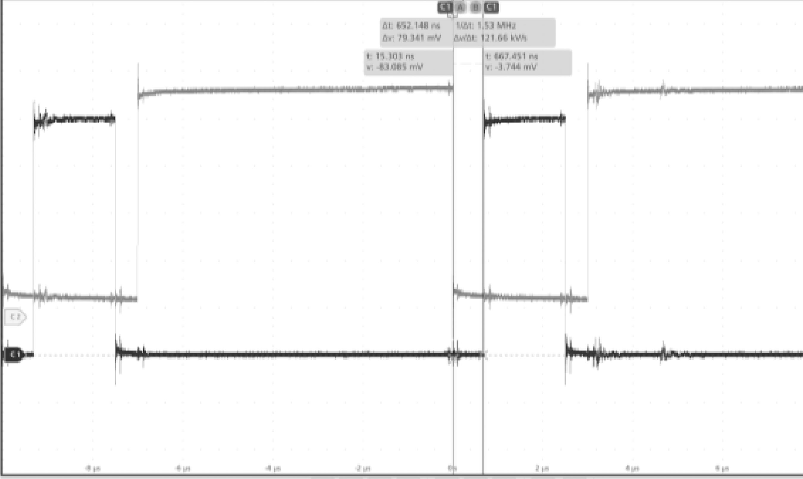
The dead time was defined using a circuit composed of logic gates and an RC network. This configuration generates a controlled delay between the HS and LS gate signals, preventing their simultaneous conduction. The resulting delay between the pulses was approximately 650 ns, see Fig. 14, ensuring safe switching and avoiding shoot-through in the half-bridge converter.

2B TEST WITH CURRENT PROBE, D = 25% and RG = 30Ω
In the second scenario, shown in Fig. 15, the voltage peak is still present. Even with RG = 30 Ω, the current measurement loop interacts with circuit parasitic inductances and transistor capacitances, resulting in oscillations, illustrated Fig. 16.
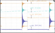
Switching waveforms with current probe and RG = 30 Ω. Vds LS and HS, Id HS, and instantaneous power HS. Horiz: 100 ns/div.
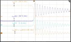
Switching waveforms with current probe and RG = 30 Ω. Vds LS and HS, Id HS, and instantaneous LS turn-on transition (b). Horiz: 100 ns/div.
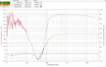
Although the voltage peak observed in the switching waveforms is not reduced when using a higher gate resistance (RG = 30 Ω), its origin is primarily associated with the interaction between the parasitic inductances of the measurement loop and the intrinsic capacitances of the MOSFET. In this operating condition, the current measurement loop introduces additional parasitic inductance in the main commutation path, which dominates the transient behavior and leads to voltage overshoots and oscillations. Therefore, the presence of the voltage peak should not be attributed solely to the gate resistance value, but rather to the combined effect of circuit parasitics and the measurement setup. This explains why increasing RG alone is insufficient to suppress the voltage peak in this scenario, despite its effectiveness in reducing high-frequency oscillations under conditions with minimized parasitic inductance. The rigid copper wire used for the drain current measurement exhibits predominantly inductive behavior, with an inductance of approximately 27 nH above 300 kHz, Fig. 17, remain stable and linear up to 30 MHz. Using the Coss capacitance (380 pF), the inductance to produce 26 MHz resonance is 100 nH, which is consistent with the inductances in the circuit.
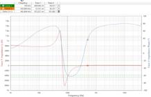
Besides the loop inductance, another point to verify is the impact of the current sensor on the loop. As shown in Fig. 18 the current probe significantly affects the characteristics in the low-frequency range, but not in the resonance range, in which the equivalent inductance remains in the range of tens of nH.
C. SWITCHING TEST WITHOUT CURRENT PROBE, D = 25% / RG= 3Ω
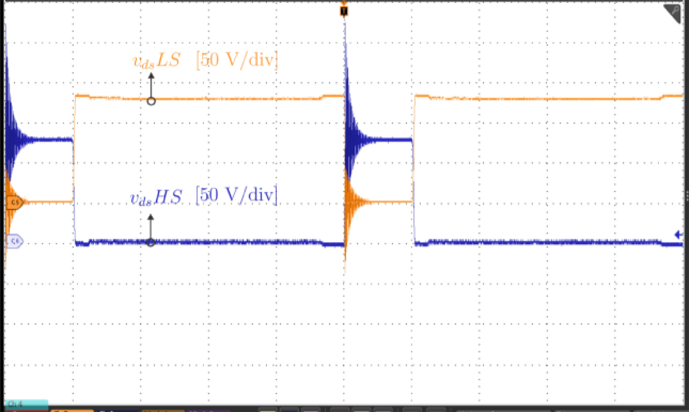
The third scenario removes the current measurement loop and reconnects the ceramic capacitors close to the MOSFET’s drain terminals, maintaining RG = 3 Ω. Fig. 19 shows the MOSFETs' Vds signals. The oscillation is still present but more damped and has a higher frequency due to the parasitic inductance reduction. The voltage peak remains high (250V peak). Since the current signal was unavailable, power analysis was no longer possible. The reverse recovery of the HS diode still causes the oscillation.
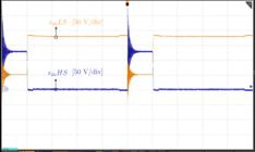
HS and LS MOSFETs Vds signals of (50 V/div), without current loop and RG = 3 Ω. Horiz: 2 µs/div.
The LS MOSFET turns off under ZVS conditions, while the oscillation arises during its turn-on phase, triggered by the reverse recovery of the HS diode. Unlike previous scenarios, the observed resonance frequency is 46 MHz, indicating a significant reduction in connection inductance, primarily due to the removal of the external current loop, the absence of the current probe, and the elimination of high-frequency bypass capacitors. Under these conditions, the total parasitic inductance is estimated to be approximately 30 nH.
FFSWITCHING TEST WITHOUT CURRENT PROBE, D = 25%, RG = 30Ω
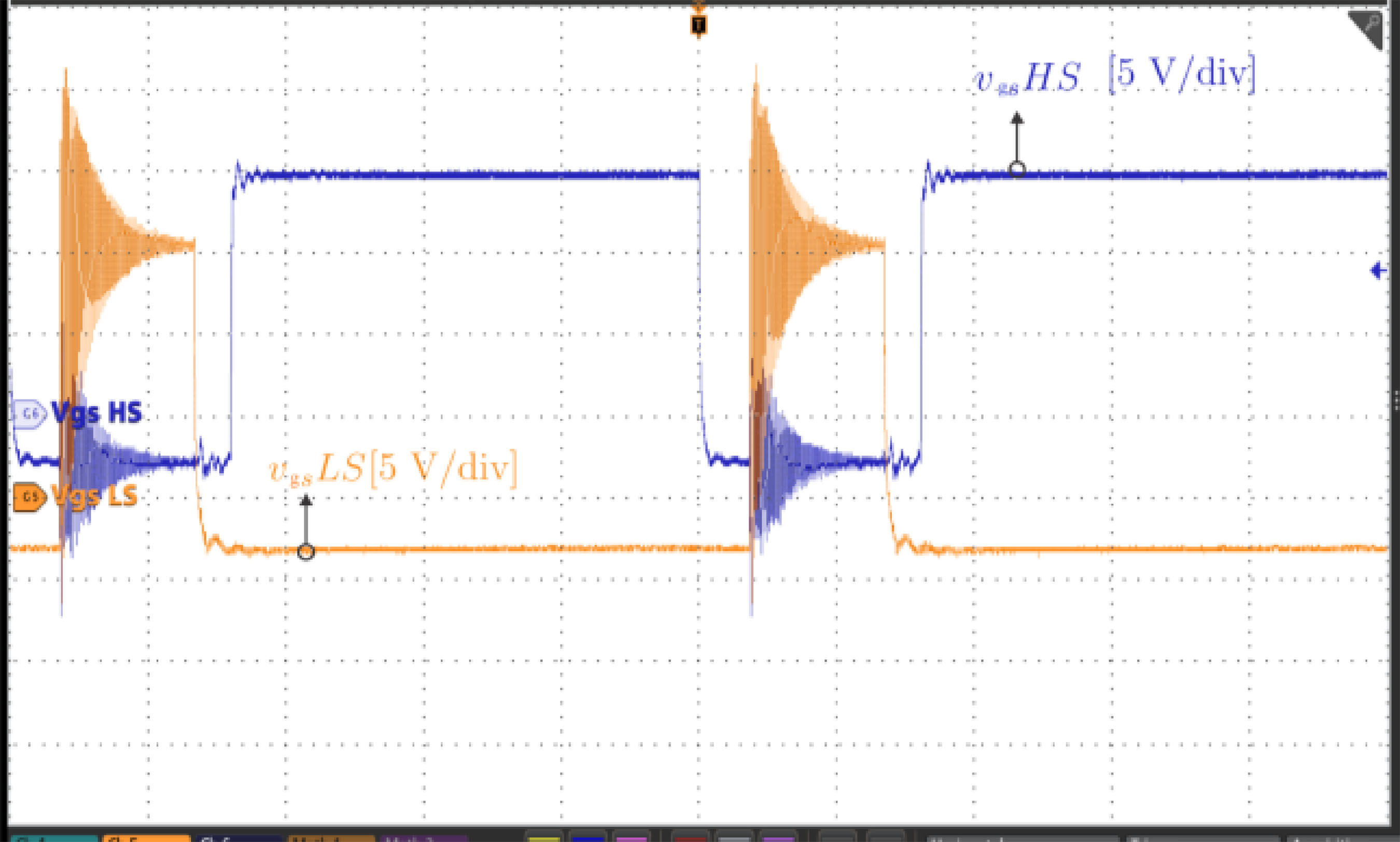
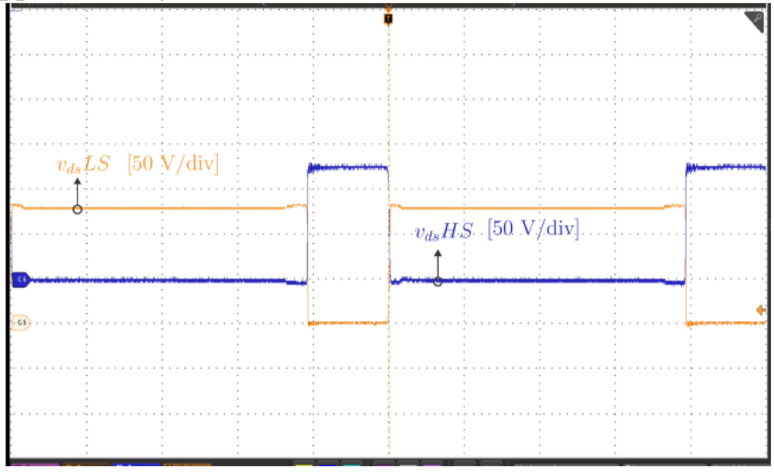
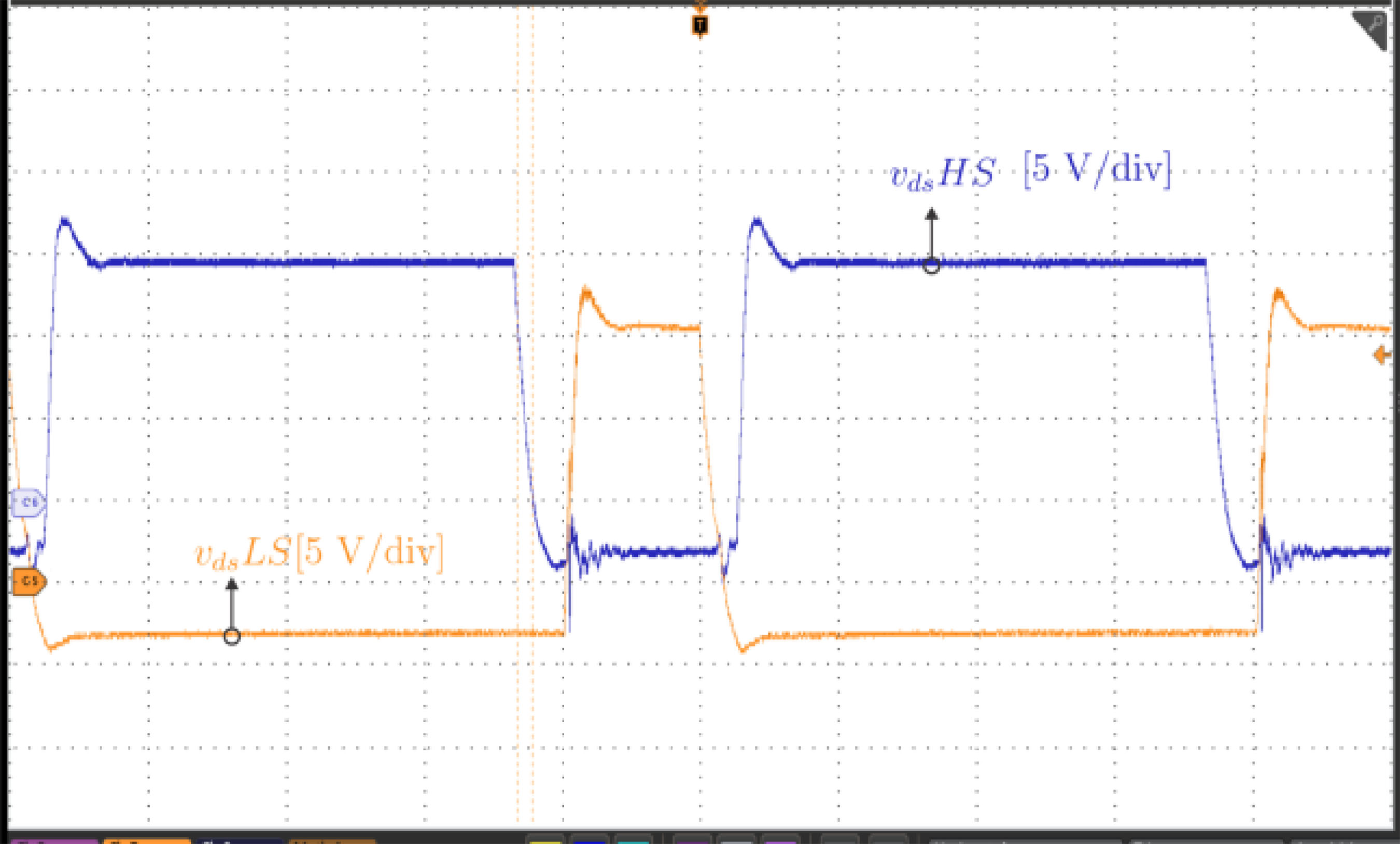
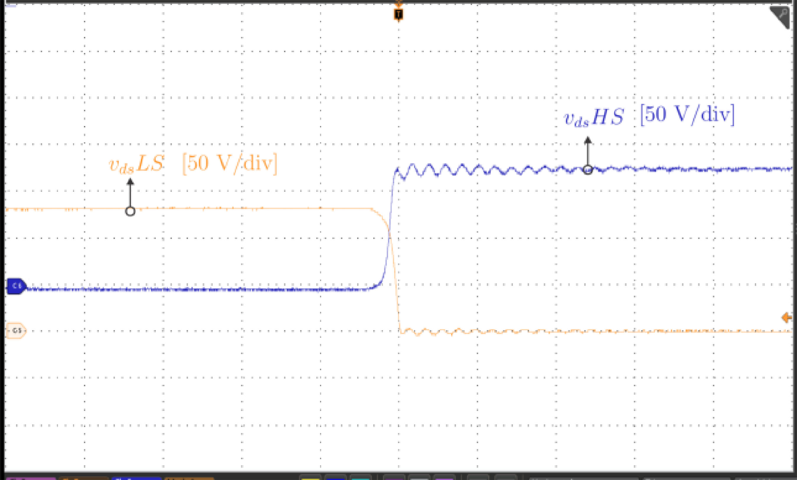
By increasing the gate resistance, the oscillations were suppressed. The Vgs oscillations were also significantly reduced, as illustrated in Fig. 18, confirming that these disturbances were primarily driven by Vds variations. Furthermore, despite a tenfold increase in gate resistance, the impact on switching speed remained negligible, as shown in Fig. 20 the MOSFETs continued to switch within approximately 30 ns.

The combined effect of increasing the gate resistance and removing the current probe, as illustrated in Figs. 21 and 22, significantly contributed to the reduction of oscillations in the switching waveforms. Increasing the gate resistance resulted in slower switching transitions, effectively limiting the excitation of parasitic inductances and capacitances that typically lead to high-frequency ringing. Simultaneously, the removal of the Hall-effect current probe minimized the additional parasitic inductance introduced by its connection loop, thereby reducing unwanted resonant interactions within the power path. Consequently, both the Vgs and Vds signals exhibited noticeably smoother transitions with diminished oscillatory behavior, improving waveform stability, reducing EMI, and enhancing the overall signal integrity of the converter.

LS and HS MOSFETs Vgs signals (5 V/div), without current loop and RG = 30 Ω. Horiz: 2 µs/div.
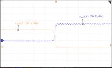
Detail of HS and LS MOSFETs Vds signals (50 V/div), without current loop and Rg = 30 Ω, at LS transistor turn-on. Horiz: 100 ns/div.
During dead-time, the output current commutes to the body diode of the MOSFET, resulting in a brief interval of diode conduction before the channel is re-established by the next gate command, see figure 23.

Body-Diode Conduction During Dead-Time ( RG = 3Ω) Vds LS 20V/div; IOUT = 1A/div; Vds HS 2V/div. Horiz: 400 ns/div.
For (RG = 3 Ω), measurements showed approximately 500 ns of diode conduction, VF = 4 V. Dissipated energy in this interval can be estimated as (E = VF × IOUT × tDEAD), and the corresponding average power is obtained by multiplying this energy by the switching frequency.
Although short, this conduction interval contributes directly to switching losses, since the diode exhibits higher forward voltage and reverse-recovery charge compared to the MOSFET channel.
IV. LOSSES ESTIMATION
The power estimation accuracy is limited by the voltage and current sensors and oscilloscope characteristics, as indicated in the Appendix.
Given this limitation, the estimation of power dissipation was carried out indirectly, through a comparison of the input and output power of the converter.
Note that these results indicate the total losses, including the non-idealities of the circuit, as the track resistance, capacitor losses, etc., not allowing one to know the contribution of each MOSFET. The tests were performed for non-ZVS.
The active power (W) is the average value of the instantaneous power over the measurement window.
A lower RG allows faster switching, reducing switching time but leading to voltage and current oscillations, increasing EMI, and causing overvoltage.
On the other hand, a higher RG slows down the transitions, which smooths the waveforms and reduces oscillations, but leads to higher dissipation. Therefore, in non-ZVS conditions, choosing the appropriate gate resistance involves balancing EMI mitigation.
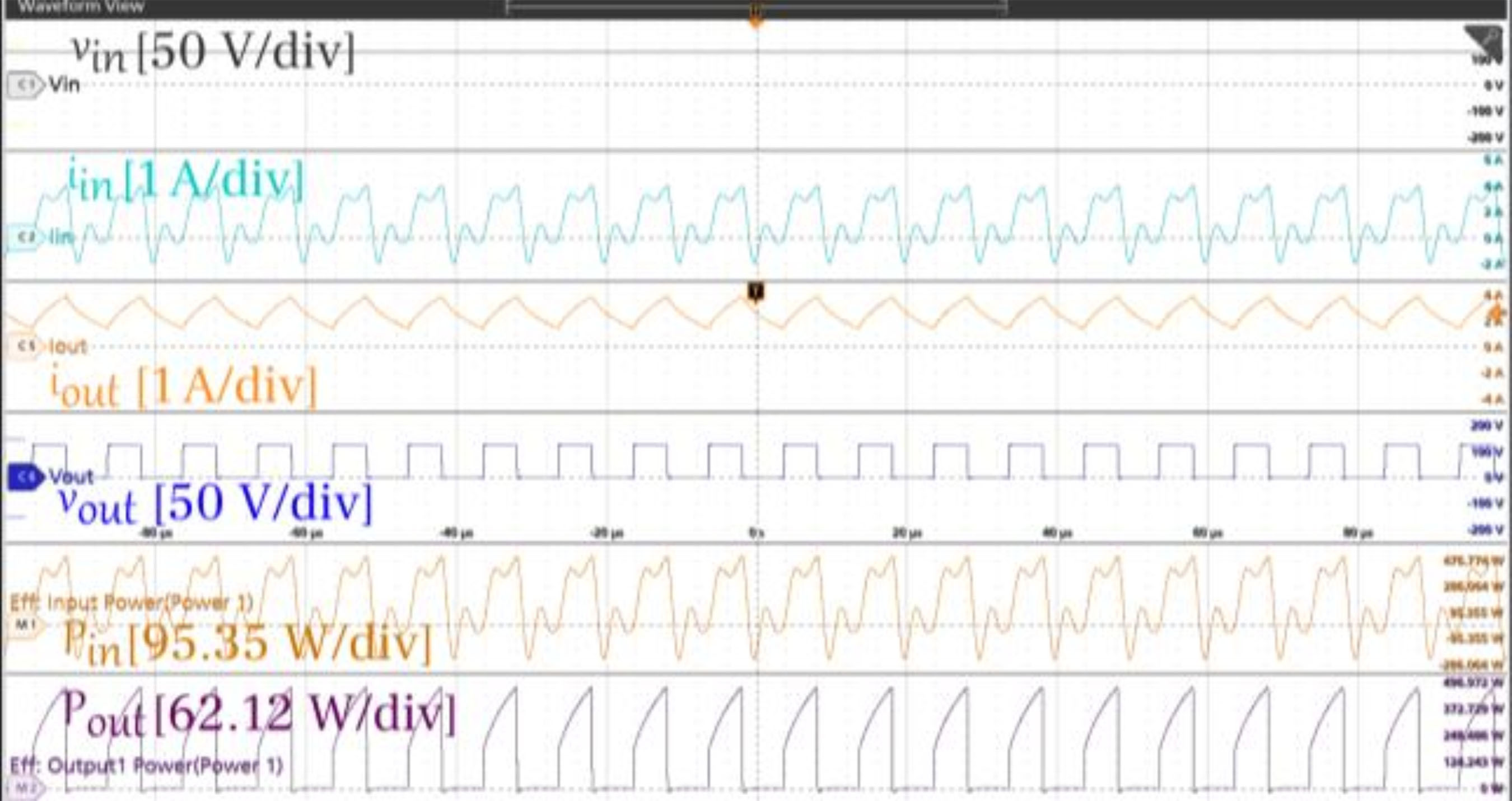
Figs. 24 and 25 illustrate the input and output voltage and current waveforms under different gate resistance values. RG = 3 Ω there are resonances inherent to the circuit, leading to oscillations. The slower switching transition damps these resonances, preventing oscillations in either the voltage or current waveforms.
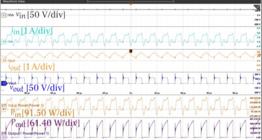
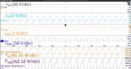
Table 5 presents the values obtained from the converter tests operating ZVS, considering two gate resistance settings: 3 Ω and 30 Ω.
Fig. 26 shows power comparison for different gate resistances. With RG = 3 Ω, the losses are 2.6 W, while with RG = 30 Ω, losses rise to 4.0 W, showing that increasing gate resistance increases losses.

Although thermal analysis was initially considered as a complementary method for validating the power loss estimation, the use of thermography in this context proved to be inconclusive. The total power difference observed between the tests, remained below 5 W. This small variation translates into a surface temperature difference of only a few tenths of a degree Celsius on the transistor capsule, well below the resolution threshold of the available thermal imaging equipment. Furthermore, accurate thermal evaluation under such low-gradient conditions would require a high-precision infrared camera and a tightly controlled ambient environment to eliminate external influences such as natural convection. Due to these practical constraints, thermographic measurements were not used as a definitive method for loss quantification in the reported results, and the loss estimation was instead based on input–output power balance, which reduced the influence of probe-induced perturbations and was more consistent with the measurement capabilities available.
V. CONCLUSIONS
In this article, an analysis demonstrated the critical influence of gate resistance and parasitic elements on switching performance, electromagnetic interference, and energy dissipation. Simulations and experimental results confirmed that fast switching in SiC devices leads to pronounced voltage and current oscillations, primarily exacerbated by diode reverse recovery and layout-induced parasitic inductances. Increasing gate resistance effectively mitigated these oscillations, but at the cost of higher switching losses, especially under non-ZVS conditions.
Experimental results confirmed that conventional current measurement techniques, particularly current probes inserted in the drain path, introduce considerable parasitic inductance that alters the converter’s dynamic behavior and compromises the accuracy of instantaneous power measurements. To overcome this limitation, the study recommends adopting non-intrusive diagnostic methods such as input–output power comparison complemented by thermal evaluation, as more reliable alternatives for switching loss estimation in high-frequency SiC-based systems. By integrating insights on the impact of gate resistance, the limitations of traditional measurement techniques, and the effectiveness of alternative diagnostic approaches, this work provides practical design guidelines that support robust, efficient, and accurate operation of next-generation converters based on wide-bandgap devices.
Ultimately, the findings highlight that optimal gate driver design in SiC-based converters must balance switching speed and electromagnetic stability. The insights gained from this study contribute to the development of robust, high-efficiency power electronics systems. Proper layout, non-intrusive diagnostics, and careful parameter tuning are essential to ensure efficient and reliable operation in high-frequency applications.
-
PLAGIARISM POLICY
This article was submitted to the similarity system provided by Crossref and powered by iThenticate – Similarity Check.
DATA AVAILABILITY
The data used in this research is available in the body of the document.
REFERENCES
-
1 B. Agrawal, M. Preindl, B. Bilgin and A. Emadi, "Estimating switching losses for SiC MOSFETs with non-flat miller plateau region," IEEE Applied Power Electronics Conference and Exposition (APEC), Tampa, FL, USA, 2017, pp. 2664-2670, doi: 10.1109/APEC.2017.7931075.
» https://doi.org/10.1109/APEC.2017.7931075 -
2“Dynamic Characterization & Measurement Methods for SiC Power Devices | Wolfspeed,” Wolfspeed.com, 2021. https://www.wolfspeed.com/knowledge-center/article/dynamic-characterization-and-measurement-methods/ (accessed May 29, 2025).
» https://www.wolfspeed.com/knowledge-center/article/dynamic-characterization-and-measurement-methods/ -
3 Y. Wei, Q. Xu, J. Hu, B. Xu, H. Wei and G. Liu, "A Hard-Switching Loss Calculation Method for SiC MOSFETs Without Current Sensors," CPSS & IEEE International Symposium on Energy Storage and Conversion (ISESC), Xi'an, China, 2024, pp. 1004-1010, doi: 10.1109/ISESC63657.2024.10785400.
» https://doi.org/10.1109/ISESC63657.2024.10785400 -
4 P. Górecki, K. Górecki and J. Rąbkowski, "Switching Energy Losses Characterization of Discrete SiC Power Transistors—A New Thermal Approach," in IEEE Transactions on Instrumentation and Measurement, vol. 74, pp. 1-11, 2025, Art no. 1504011, doi: 10.1109/TIM.2025.3555731.
» https://doi.org/10.1109/TIM.2025.3555731 -
5 D. Rothmund, D. Bortis and J. W. Kolar, "Accurate Transient Calorimetric Measurement of Soft-Switching Losses of 10-kV SiC mosfets and Diodes," in IEEE Transactions on Power Electronics, vol. 33, no. 6, pp. 5240-5250, June 2018, doi: 10.1109/TPEL.2017.2729892.
» https://doi.org/10.1109/TPEL.2017.2729892 -
6 J. A. Anderson, C. Gammeter, L. Schrittwieser and J. W. Kolar, "Accurate Calorimetric Switching Loss Measurement for 900 V 10 m $\Omega$ SiC mosfets," in IEEE Transactions on Power Electronics, vol. 32, no. 12, pp. 8963-8968, Dec. 2017, doi: 10.1109/TPEL.2017.2701558.
» https://doi.org/10.1109/TPEL.2017.2701558 -
7 A. Anurag, S. Acharya, Y. Prabowo, G. Gohil, H. Kassa and S. Bhattacharya, "An accurate calorimetric method for measurement of switching losses in silicon carbide (SiC) MOSFETs," IEEE Applied Power Electronics Conference and Exposition (APEC), San Antonio, TX, USA, 2018, pp. 1695-1700, doi: 10.1109/APEC.2018.8341245.
» https://doi.org/10.1109/APEC.2018.8341245 -
8 A. Anurag, S. Acharya and S. Bhattacharya, "An Accurate Calorimetric Loss Measurement Method for SiC MOSFETs," in IEEE Journal of Emerging and Selected Topics in Power Electronics, vol. 8, no. 2, pp. 1644-1656, June 2020, doi: 10.1109/JESTPE.2019.2920935.
» https://doi.org/10.1109/JESTPE.2019.2920935 -
9 Q. Yang, A. Nabih, R. Zhang, Q. Li and Y. Zhang, "A Converter Based Switching Loss Measurement Method for WBG Device," IEEE Applied Power Electronics Conference and Exposition (APEC), Orlando, FL, USA, 2023, pp. 8-13, doi: 10.1109/APEC43580.2023.10131509.
» https://doi.org/10.1109/APEC43580.2023.10131509 -
10 M. Mandal, B. K. M, M. G, S. K. Roy and K. Basu, "Energy-based Method to Estimate the Partial Hard Turn-on Loss of Complementary SiC MOSFET from Experiment," IEEE Applied Power Electronics Conference and Exposition (APEC), Long Beach, CA, USA, 2024, pp. 1114-1119, doi: 10.1109/APEC48139.2024.10509333.
» https://doi.org/10.1109/APEC48139.2024.10509333 -
11 D. Nayak, Y. Ravi Kumar and S. Pramanick, "A Comparative Study of Loss Measurement Techniques for SiC MOSFET Based PE Converters," 48th Annual Conference of the IEEE Industrial Electronics Society, Brussels, Belgium, 2022, pp. 1-6, doi: 10.1109/IECON49645.2022.9968884.
» https://doi.org/10.1109/IECON49645.2022.9968884 -
12 U. Das, M. Mandal, S. Ghotgalkar and K. Basu, "Experimental Method for Accurate Measurement of High Frequency Bridge Loss," IEEE International Conference on Power Electronics, Drives and Energy Systems (PEDES), Mangalore, India, 2024, pp. 1-6, doi: 10.1109/PEDES61459.2024.10961456.
» https://doi.org/10.1109/PEDES61459.2024.10961456 -
13 F. M. Ribeiro, R. Heinrich, and Y. R. Novaes, “Minimização dos efeitos de elementos parasitas em circuitos de Double Pulse Test para GaN HEMT”, Eletrônica de Potência, vol. 30, p. e202541, Jul. 2025, doi: 10.18618/REP.e202541.
» https://doi.org/10.18618/REP.e202541
APPENDIX
The instrumentation used for signal measurements in circuits employing SiC MOSFETs must ensure high precision, galvanic isolation, and sufficient bandwidth. Accurate signal acquisition is critical in these applications due to the high switching speeds, elevated voltages, and fast transient events typical of WBG semiconductors.
During the development and testing of SiC-based half-bridge converters, various oscilloscope models and probes were evaluated to identify the most suitable configuration. Simpler or lower-bandwidth oscilloscopes were tested and found to produce signal distortion, false transients, and inaccurate interpretation of switching behavior. These distortions compromise the analysis of critical parameters such as rise time, overshoot, and ringing, potentially leading to incorrect design decisions or overlooked reliability issues.
After comparative testing, the Tektronix MSO46 was selected as the main measurement platform due to its superior performance. With a bandwidth of 500 MHz and a sampling rate of 6.25 GSa/s, this oscilloscope offered the necessary temporal resolution and accuracy for capturing fast switching events in WBG devices. It was used in conjunction with a signal generator (Siglent SDG 1032X) and various voltage and current probes across all test scenarios.
For voltage measurements, the Tektronix THDP0200 differential high-voltage probe was used. It provides a bandwidth of 200 MHz and can measure up to 1500 V, offering good isolation and response for high-voltage circuits. In the test environment, it achieved a rise time of 3.93 ns and a signal delay of 8.94 ns, using the Tektronix TPP0500B as a passive reference probe. While it performed well, some limitations, such as electromagnetic coupling and noise sensitivity, were observed.
To measure current, the Tektronix TCP0030A current probe was employed. It has a bandwidth of 120 MHz and a maximum measurement capability of 30 A. Using the Hall effect, it converts the magnetic field into a voltage signal. During testing, it demonstrated a rise time of 483.6 ns and a signal delay of 165 ns, with performance comparable to other commercial current probes, such as the Yokogawa 701933.
In conclusion, after extensive testing with multiple oscilloscope and probe models, the Tektronix MSO46 combined with the THDP0200 and TCP0030A probes was proven to be the most reliable and accurate configuration. For SiC-based power electronics, especially in fast-switching environments, using high-performance instrumentation is critical to avoid signal distortion and ensure trustworthy data for design validation.
Edited by
-
The review of this paper was arranged by Associate Editor Victor F. Mendes https://orcid.org/0000-0002-8453-344X and Editor-in-Chief Allan F. Cupertino https://orcid.org/0000-0001-8418-1985.
History
-
Received
28 Aug 2025 -
Reviewed
17 Nov 2025 -
Reviewed
11 Dec 2025 -
Accepted
18 Dec 2025 -
Published
19 Jan 2026