Modeling and Validation of Junction Temperature Estimation in High-Power SiC MOSFET Inverters for Electric Vehicle Applications
ABSTRACT
The growing concern with reducing CO2 emissions and the demand for sustainable mobility have promoted the adoption of electric vehicles and the use of wide bandgap semiconductors. Thermal management for semiconductor devices is crucial to ensure reliability and efficiency, with junction temperature being a key variable that cannot be directly measured during operation. In this context, this paper proposes a method for junction temperature estimation of SiC MOSFET devices applied to electric traction inverters. A Luenberger state observer is applied to estimate the junction temperature from accessible variables such as ambient temperature, heat sink temperature, and calculated power losses. The method is formulated in a state-space representation, verified through simulations, and validated using an experimental setup, consisting of a single-phase full-bridge inverter. Infrared thermal imaging and physical sensors were employed to compare estimated and measured values. The results demonstrated high accuracy and fast dynamic response of the proposed observer, confirming its robustness and applicability for embedded thermal monitoring in power converters.
KEYWORDS
Embedded thermal monitoring; thermal modeling; state observer; wide bandgap semiconductors; electric traction inverters
I. INTRODUCTION
Electrical Vehicles (EVs) are emerging as protagonists in the context of sustainable technological progress due to its capacity of operation without tailpipe carbon emissions Replacing the traditional internal combustion engine vehicle fleet for EVs can provide substantial decrease in the carbon emissions, whichs contributes for the global goal of decarbonization. A crucial component in the development and operation of a EV is the traction inverter. This device is responsible for controlling the energy flux of the battery to the motor and sometimes for battery charging [1]. As the industry moves towards electrical traction systems, the demand for smaller, more efficient and high-power-density inverters grows. These demands are linked not only by the necessity of space restrictions and vehicle weight, but with the need of provide dynamic driving cycles with high reliability. In this context, SiC Mosfet have been increasingly used in several commercial traction inverters developed by automotive manufacturers. One of the main challenges regarding the adoption of SiC Mosfets is the monitoring or direct measurement of junction temperature of these devices. The direct measurement approach is invasive and often impractical due to the constructive limitations of the components [2]. Moreover, solutions based on dedicated sensors present high cost and are faultsusceptible [3].
Several indirect approaches for estimating junction temperature have been explored, typically combining the analysis of electrical parameters with equivalent thermal models. In [4], a measurement-informed thermal model is proposed that enables junction-temperature estimation even when key parameters are unknown. Among these approaches, a second-order estimator achieved the best performance, delivering high accuracy and efficiency, particularly for active thermal control. In [5], the authors present a comprehensive review of thermal models and thermal-management strategies for power semiconductor devices, with a focus on measuring and estimating the junction temperature of insulated-gate bipolar transistors (IGBTs). In this work, Cauer and Foster-type equivalent thermal networks are discussed to represent the thermal behavior of power devices, and three methods for determining junction temperature are evaluated: optical, physical, and electrical. According to the review, although optical and physical techniques can offer high resolution, they are generally unsuitable for online measurements, especially when the chip is not visible.
In [6], the authors propose implementing Kelvinemitter sensing directly on the aluminum substrate, at the emitter surface of the IGBT module, with potential applicability to power Mosfet modules as well. In [7] the authors presented a reduced-order observer coupled with a disturbance estimator to monitor the power module temperature. This approach minimizes errors caused by parameter and operating condition uncertainties, providing a real-time estimation of the junction temperature. The paper [8] proposed a virtual sensor based on the Luenberger observer to estimate the junction temperature in closed-loop systems. The methodology combines 3-D simulations and experimental validation to demonstrate the observer’s performance, highlighting its robustness against system perturbations. In the [9], a full-order observer with online method to estimate the junction temperature of the IGBT device. The strategy employed is valid to devices with multilayer structures. The observer proved to be more robust than other methods based on thermal modeling, since its feedback matrix can compensate for errors caused by parameter inaccuracies and uncertainties in the initial states. The proposed approach was validated through simulations using finite element analysis (FEA) and practical experiments. [10] proposed an estimation of the junction temperature using RC thermal networks, where the parameters were experimentally identified by varying the ambient and cooling liquid temperatures.
Paper [11] compared two methods for estimating thermal states, both based on thermal model nonlinearities combined with a Kalman filter. The first method relies on measurements from an NTC sensor integrated into the modules, assuming steady-state conditions, while the second method employs an additional sensor to measure the inlet temperature of the cooling fluid, providing higher accuracy under dynamic operating regimes. [12] developed a model-based Luenberger observer to estimate the IGBT junction temperature, in which a linear model with variable parameters was proposed as a function of the cooling and hydraulic systems.
This paper proposes a method for estimating the junction temperature of SiC MOSFET devices using a Luenberger observer driven by ambient temperature, cooling system temperature, and calculated power. The approach is validated through both simulation and experimental results. A single-phase full-bridge converter was used for experimental validation. The main contribution of the paper is the proposal of a methodology for junction temperature estimation of SiC Mosfet inverters. In contrast to most studies in the literature, which rely solely on simulations or intrusive sensing techniques, the proposed method combines analytical power-loss modeling, simplified thermal modeling, and an observerbased estimation strategy implemented directly in hardware. Experimental validation using thermal cameras and embedded sensors demonstrates that the proposed observer provides faster and more accurate tracking of the junction temperature than the built-in module sensor. These results highlight the potential of the approach for embedded thermal monitoring in traction inverters, enabling reliable estimation with reduced sensor count and low implementation cost.
II. MODELLING OF THERMAL SYSTEM
A. Power losses calculation
In this paper, a full-bridge converter is adopted to validate the proposed junction temperature estimation approach. In this type of converter, the instantaneous power losses can be assumed to be composed of conduction losses (PC) and switching losses (PSW). The diode losses can be neglected since the diodes conduct for a very short time intervals, which are negligible compared with the losses in the Mosfet switches [13]. Therefore, the total losses PTOT for each switch can be obtained from the sum of PC and PSW. This expression will be further used for the observer inputs Ploss,U and Ploss,D in section III.F.
1) Conduction losses
When the Mosfet is carrying current, the instantaneous losses can be obtained from expression (2), which is basically the product of the drain current ID with the drain-source resistance RDS(on), considering the duty cycle d,
The drain-source resistance depends of the junction temperature and can be calculated as
where
In this way, the MOSFET resistance is not constant and changes with the junction temperature. This behavior shows the need for a dynamic modeling for the conduction losses, in which RDS(on) is constantly updated in respect to the device temperature, vide Section III. This strategy allows for more realistic estimation of losses, especially during load transients. This approach becomes even more relevant in applications with significant thermal stress, such as vehicle traction, where the thermal performance has a direct influence in the system reliability [14].
2) Switching losses
In this work, the equation for Mosfet switching losses was based in [15], where the authors propose a simplified and practical approach for thermal estimation in power converters with inductive load. The adopted equation is given by,
The expression is divided into two terms, each with a clear physical meaning. The first term represents the energy dissipated during the switching process, assuming linear voltage and current waveforms during device commutation. In this formulation, ton corresponds to the turn-on time, associated with the simultaneous rise of the current and fall of the voltage (rise time), whereas toff represents the turn-off time, during which the current falls and the voltage rises (fall time). Under this assumption, the energy is computed as the triangular area under the current and voltage curves, providing an estimation of the dissipated energy in each switching cycle. In this term, the drain current ID, the DC-bus voltage VCC, and the switching frequency fsw are considered variables.
The second term corresponds to the energy stored in the device’s output capacitance COSS, which is released during MOSFET turn-on. Although this energy is not directly evident in the voltage and current waveforms, it contributes significantly to the device’s internal temperature rise. The implicit inclusion of this term enables a more accurate estimation of dynamic losses, particularly in high-voltage and high-frequency applications, which are typical operating conditions for SiC Mosfets [15]. The calculation of the switching times ton and toff is based on the method presented in [16].
B. System description
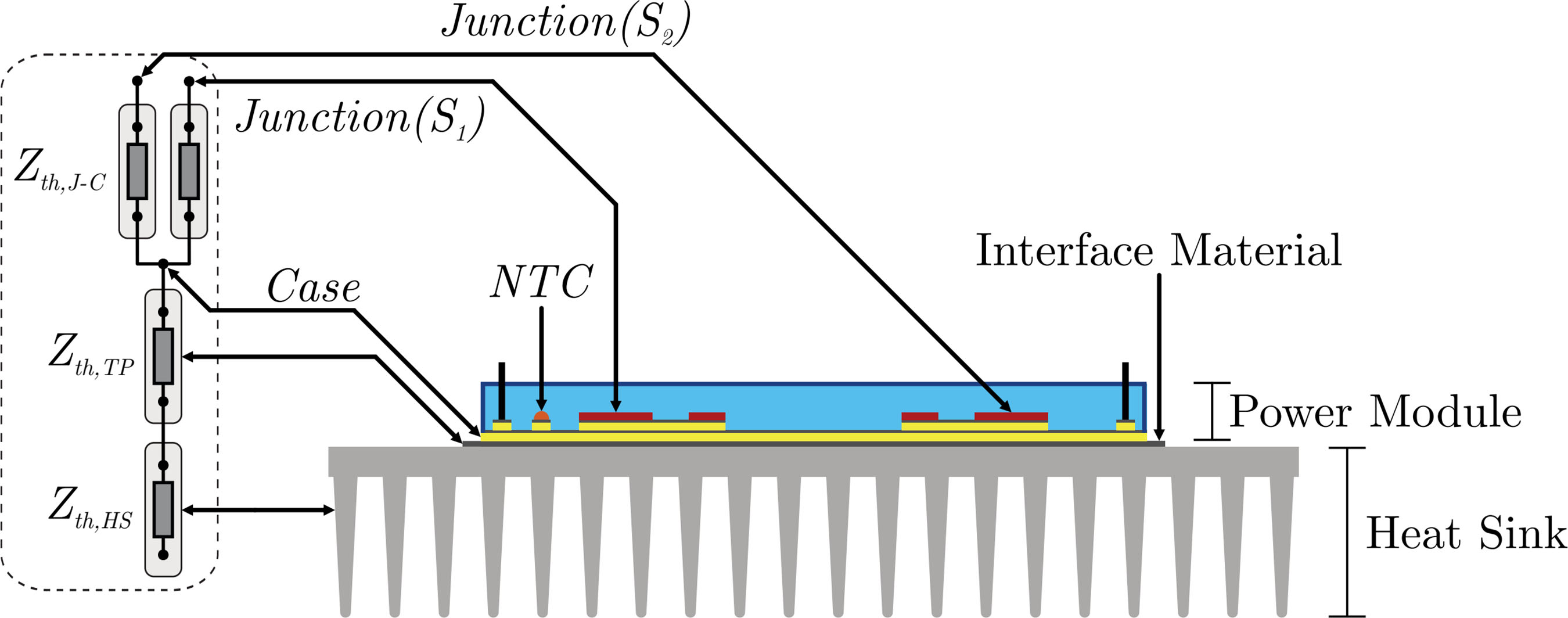
In this paper, a full-bridge inverter was selected to implement and test the proposed observer. This system uses a natural convection cooling system. The typical structure of a thermal cooling system is presented in Figure 1. This figure shows the base cooling system, thermal paste, and the SiC Mosfet device.
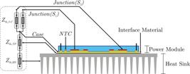
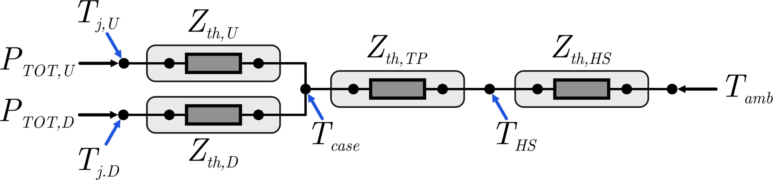
From Figure 1 it is possible to build an equivalent electric circuit that models the thermal system. Thus, a dynamic model based on thermal impedances can be derived to describe the hot spots in the semiconductor module. In order to simplify the thermal system modelling, Figure 2 presents the thermal sequence, where the inputs correspond to the power losses of each power module and the ambient temperature. This representation reduces the effort required to define the equivalent RC network of the system.
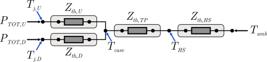
The figure illustrates the thermal impedances of the equivalent model, showing the main variables of interest in the system. The total losses obtained by the sum of: PTOT,U and PTOT,D, that are generated respectively by the upper and lower devices of the power module, constitute the heat sources of the system. These losses propagate through the thermal impedances Zth,U and Zth,D, associated with thermal impedance of each device, resulting in the junction temperatures Tj,U and Tj,D. The global impedance Zth,TP represents the thermal path between the module case (Tcase) and the heatsink (THS), including the interface material, in this case, the thermal grease. Finally, the impedance Zth,HS describes the thermal dynamics of the heatsink in relation to the ambient temperature (Tamb).
C. Equivalent Thermal Modeling of a Full-Bridge Inverter
The number of RC elements in the thermal network directly determines the order of the resulting dynamic system. Increasing the number of capacitive and resistive blocks raises the model order and, consequently, leads to a more complex dynamic response Higher-order systems allow a more accurate representation of the different thermal response times across the module layers, capturing both the fast temperature variations at the junction and the slower responses of the heat sink. On the other hand, reduced-order models provide lower fidelity but offer advantages in terms of computational simplicity and ease of real-time implementation.
In the equivalent thermal modeling, the heat sink was represented by an RC network in order to capture the thermal dynamics of the metallic body. The presence of the capacitance is essential to model heat retention over time, while the thermal resistance reflects heat conduction to the ambient. On the other hand, the thermal paste was modeled as a pure resistance, since its mass and thermal capacity are negligible compared to the other elements, and its main function is to provide a conductive path between the package and the heat sink [17].
D. Equivalent Thermal network
As described in the previous section, the internal thermal impedance of the SiC MOSFET MSCSM70AM10CT3AG power module was obtained from the manufacturer’s data [18], originally provided as a 7th-order Foster network. The choice of this module is motivated by the advantages of wide bandgap (WBG) devices, such as higher thermal conductivity, lower switching losses, and improved efficiency under high-frequency operation, making it suitable for traction inverter applications. To facilitate practical implementation and reduce computational burden, the network was simplified by directly combining RC pairs, yielding a third-order model. This reduced structure was then converted into the Cauer topology, enabling proper interconnection with the remaining thermal blocks.
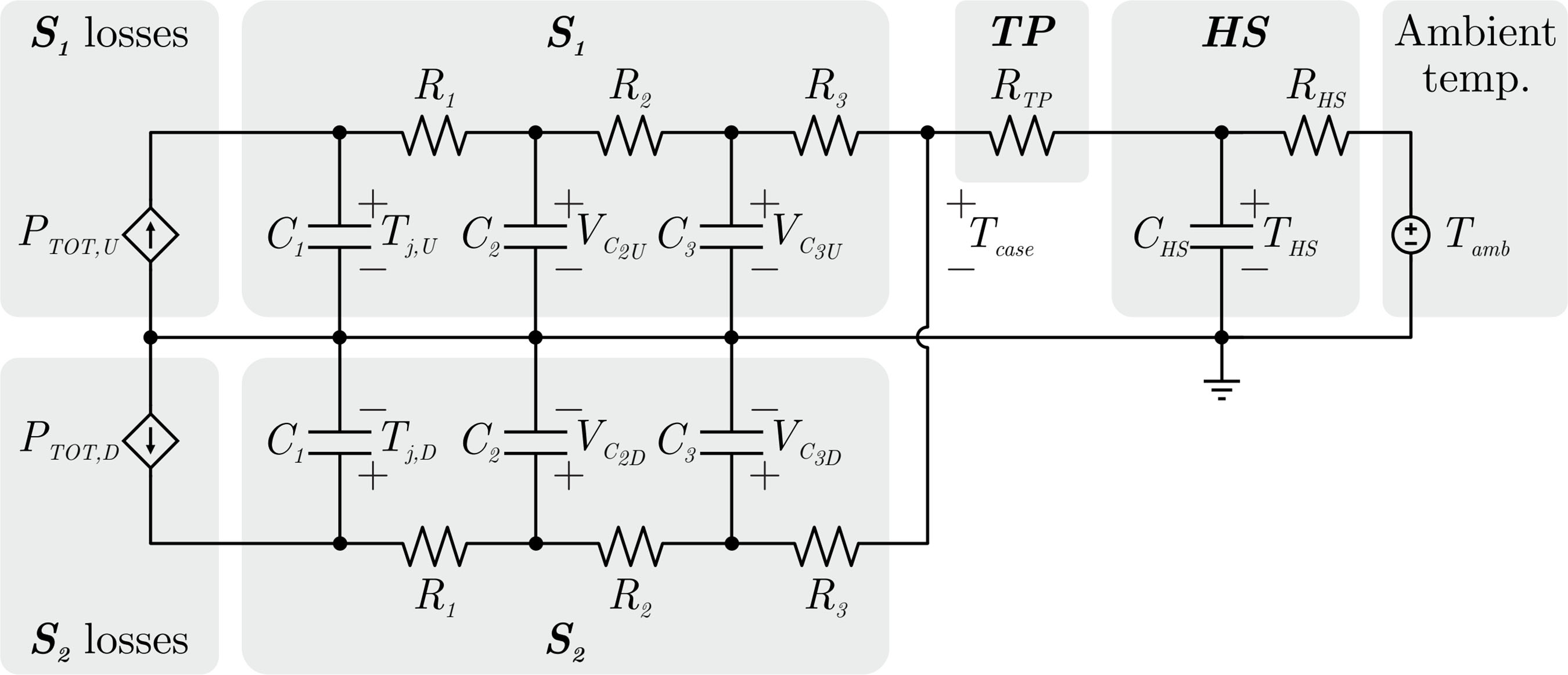
These simplified thermal networks, which represent a complete thermal model of a single power module, are shown in Figure 3. The module separately accounts for the power losses of the two semiconductors and includes the junction, case, and heat sink temperatures. This representation is used to model the thermal system and to analyze its dynamic behavior.
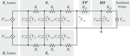
In addition to the previously defined variables, the complete thermal network includes the dynamics of the heatsink through a first-order RC system, with the thermal capacitance CHS and resistance RHS. The thermal interface material, since it has no dynamics, is modeled only by its thermal resistance RTP. The reducedorder Cauer network is represented by the RC branches (R1,C1), (R2,C2), and (R3,C3), which capture the transient thermal behavior of the semiconductor devices, with equivalent values assigned to both switches of the module. The voltages across the capacitors, VC2U and VC3U for switch S1, and VC2D and VC3D for switch S2, are analog representations of the intermediate thermal node temperatures associated with each devices in the module.
The method implemented in this work, which considers natural convection cooling, represents the ambient temperature by means of a voltage source. This approach is common in thermal modeling based on electrical analogies, as it allows defining a thermal reference and, consequently, establishing the temperature gradient across the equivalent network.
For high power levels, temperature management becomes a critical concern. In such cases, the thermal model can be directly adapted by replacing the voltage source representing ambient temperature with the coolant temperature in the equivalent thermal network. This strategy, employed in [11], accurately captures the thermal gradients that influence the junction temperature, particularly during transient conditions. Such an adaptation is especially useful in systems with high heat flux, as well as in SiC Mosfet–based converters, which operate with high power density and demand effective thermal control.
With the complete definition of the equivalent thermal circuit, the heat transfer dynamics throughout the system can now be mathematically described. This representation establishes the foundation for deriving an analytical model capable of estimating the junction temperature in real time. The next subsection presents the mathematical formulation of the thermal network, enabling a compact and accurate description of its transient behavior.
E. Thermal network modeling
The thermal network presented consists of seven layers, corresponding to a seventh-order thermal model, in which the power losses are modeled as current sources and the ambient temperature is represented by a voltage source. The junction temperatures of the upper and lower semiconductor devices are represented by capacitor voltages distributed along the physical structure of the module, while the thermal node THS corresponds to the heatsink temperature, referenced to the ambient condition. The thermal parameters of the original seventh-order model of of each switch are defined by the thermal resistances Rth = {5.0, 56.0, 13.0, 51.0, 9.0, 55.0, 30.0} mΩ and thermal capacitances Cth = {0.8, 0.0536, 0.6154, 0.5686, 2.8889, 0.1636, 1.83}.
To enable a computationally efficient implementation, suitable simplifications and mesh associations are then applied, resulting in an equivalent third-order thermal model that preserves the dominant thermal dynamics of the original network. This reduced-order representation is subsequently adopted for real-time implementation.
The resulting thermal model can be described by a set of first-order ordinary differential equations obtained through the application of the thermal node method. Each equation governs the temporal evolution of a specific temperature state associated with the thermal network, thereby providing a suitable framework for dynamic analysis and observer-based temperature estimation. Then, from Figure 3 is it possible to obtain the following differential equations,
where the auxiliary variable is given by:
Above equations were formulated in the continuous domain and can be represented in state space, enabling direct implementation in computational simulations as well as the analysis of the thermal step response as a function of power losses and the system’s thermal boundary conditions.
F. State-Space Representation of the Thermal Network
Based on the differential equations defined in the previous subsection, the thermal model of the semiconductor module can be expressed in state-space form. This representation is useful for dynamic analysis and for computationally efficient implementation in simulations or real-time control. The matrix structure also enables the application of classical techniques for linear systems, such as step-response verification. Then, the thermal system is represented by the following equation,
where x ∈ R7 represents the variables vector composed by the voltage capacitors equivalents; u ∈ R3 there are inputs of the system like the power losses of the semiconductors and the ambient temperature. y represents the output system, which is the heat sink temperature. The matrix K contain the capacitance associated each space of state, while A represents the thermal interaction between the nodes and B relates the inputs with nodes the system. Thus,
and the input vector is given by,
Matriz K is given by,
Matriz A relates the thermal interactions among the different nodes of the network. In order to simply the system the following auxiliary expressions were adopted:
which results in,
and,
The input matriz B is defined as,
and, finaly the output matriz C was selected in order to define as output the heat sink temperature, such as,
This state-space structure enables the simulation of the system’s thermal response under different power loss profiles and ambient temperature conditions. It also enables the integration with complete electrothermal models or with thermal control strategies based on dynamic temperature estimates.
III. JUNunction temperature observer
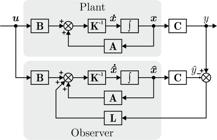
In this work, a Luenberger observer based on the statespace thermal model developed in Section F is developed. This observer is based on the use of the heat sink temperature measurement to feedback the estimated trajectory of the internal system’s thermal states. The observer model is defined as:
where the variables with the symbol ∧ represent the system’s thermal states estimation. The estimated output yˆ is obtained through the estimated state-space vector xˆ via the previously defined C matrix. The matrices K, A and B follow the same structure established in the statespace representation, and L represents the observer gain vector, which is designed to minimize the error between the estimated output yˆ and the measured output y. The observed output is stabilized via:
In this way, the heat sink temperature TˆHS is used in the state-space feedback, because it is the only thermal quantity accessible during operation. The observer operates by correcting the internal states xˆ error estimation, especially the junction temperatures Tˆj,U and Tˆj,D based on the discrepancy between the stimated value yˆ and the real value y.
The gain vector L is defined to act exclusively in the heat sink temperature THS, beeing zero in the other elements:
In this way, the 7th vector state xˆ is directly corrected by the error between the estimated output TˆHS and the measured output THS. Therefore, the other internal variables estimation, as the junction temperatures, are indirect influenced by the thermal model dynamic, since the states are interconnect by the matrices A and K.
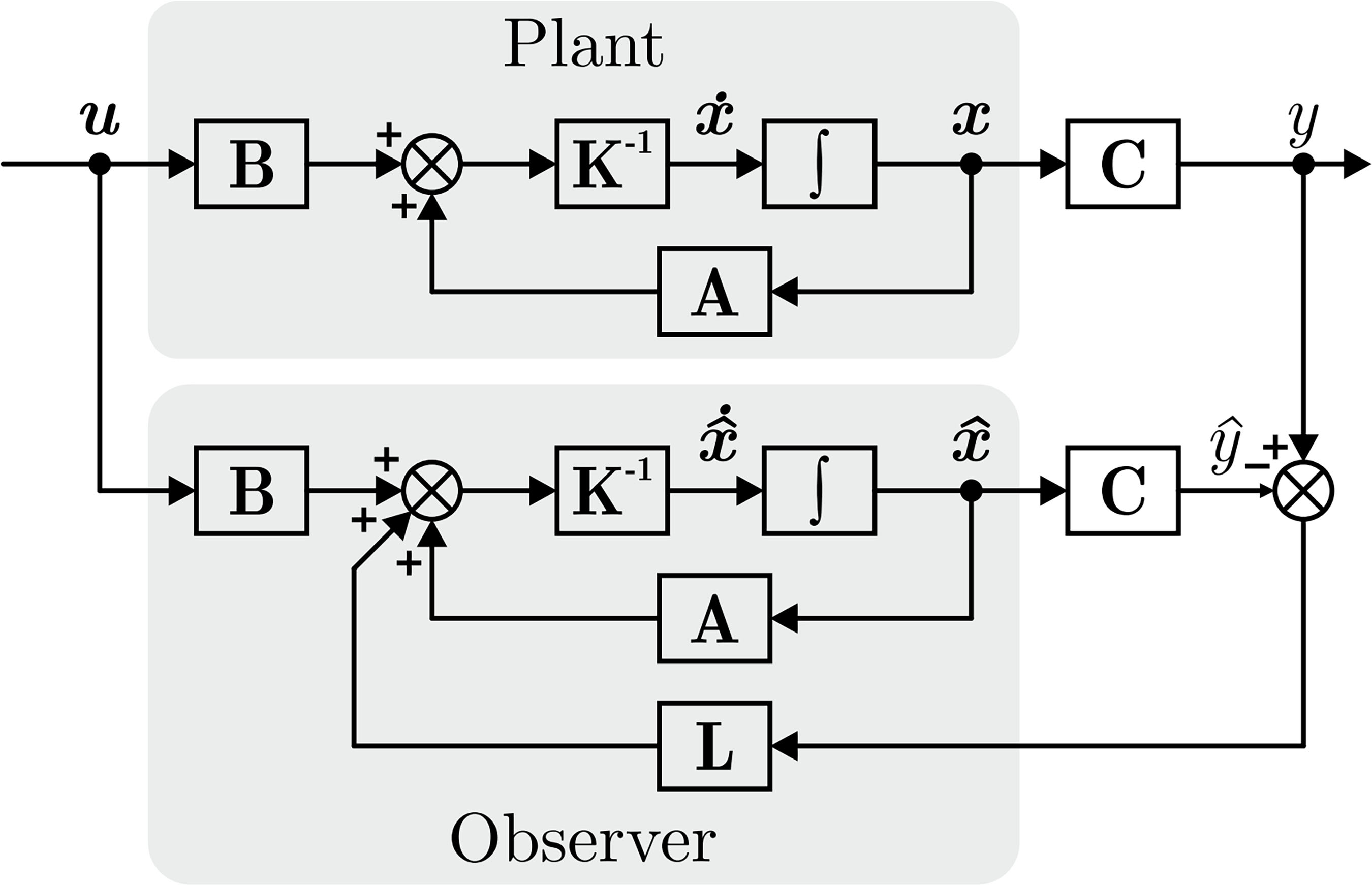
Figure 4 depicts the complete block diagram of the modeled system, integrating the state-space thermal model and the Luenberger observer implemented for the junction temperature estimation. The diagram highlights the thermal plant structure, as the corrective feedback based on the output error (y − yˆ). The position for the inverting matrices K blocks highlights the consistence with the physics model formulation, ensuring that the thermal dynamic properly considers the system’s thermal capacitances.
With the completely defined thermal modeling structure, including the characterization of instantaneous losses, building equivalent thermal networks, and statespace formulation with a state observer, the theoretical foundation for system analysis is complete. The following chapter presents the results, with emphasis on dynamic simulations, performance evaluation, and validation of the proposed temperature estimation method.
IV. Results and discussion
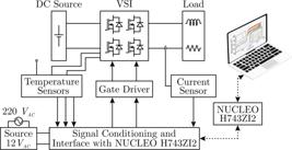
Simulation and experimental results are presented to validate the effectiveness of the proposed junction temperature estimation method in high-power inverters for vehicular applications. The objective is to demonstrate the estimator’s capability to follow the thermal dynamics of the device, ensuring robustness against load variations and operating conditions, with the possibility of enabling protection strategies for the system. In this context, the consistency between the simulated and experimental responses is evaluated, verifying the practical applicability of the approach. Figure 5 presents the representation os the simulated and actual experimental setup.
A. Simulation results
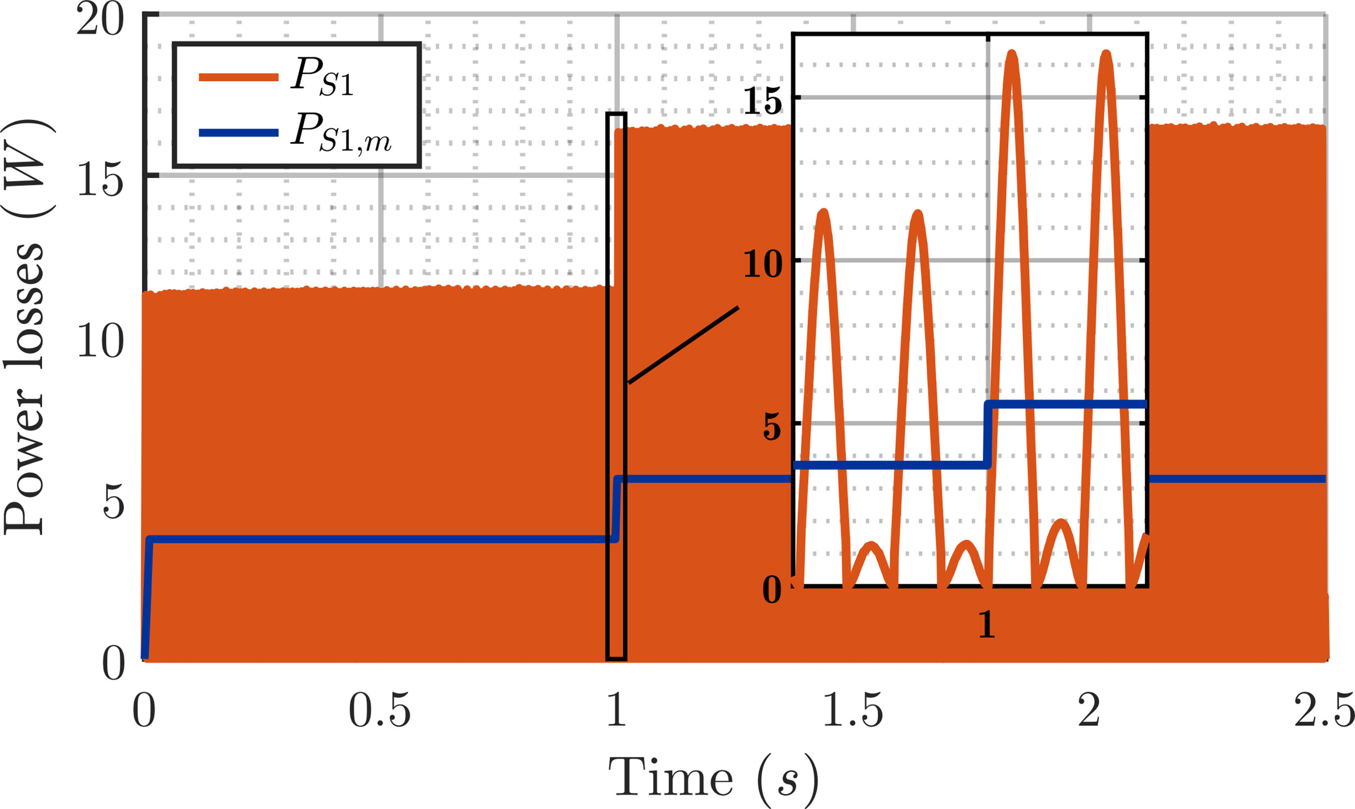
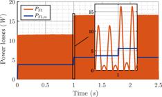
Simulation results in this section aim to verify the effectiveness of the Luenberger observer. The observability analysis is carried out by comparing the plant response with the estimated values for different observer gain configurations. To verify the thermal dynamics of the modelled system a simulation is carried out. An RL load is driven by a full-bridge SiC inverter. During the first interval (0–1 s), the load current is kept at 15 A rms, and at 1 s it is increased to 20 A rms. Figure 6 shows the inverter switch losses of the previous simulation. The figure illustrates the power losses in the upper device (S1) during a load step. The orange curve (PS1) corresponds to the instantaneous power, showing the high-frequency fluctuations associated with the switching operation, while the blue curve (PS1,m) represents the average losses, which are the main contributors to the thermal dynamics. This result confirms the consistency between the load variation and the estimated thermal losses, which serve as input for the equivalent thermal model.
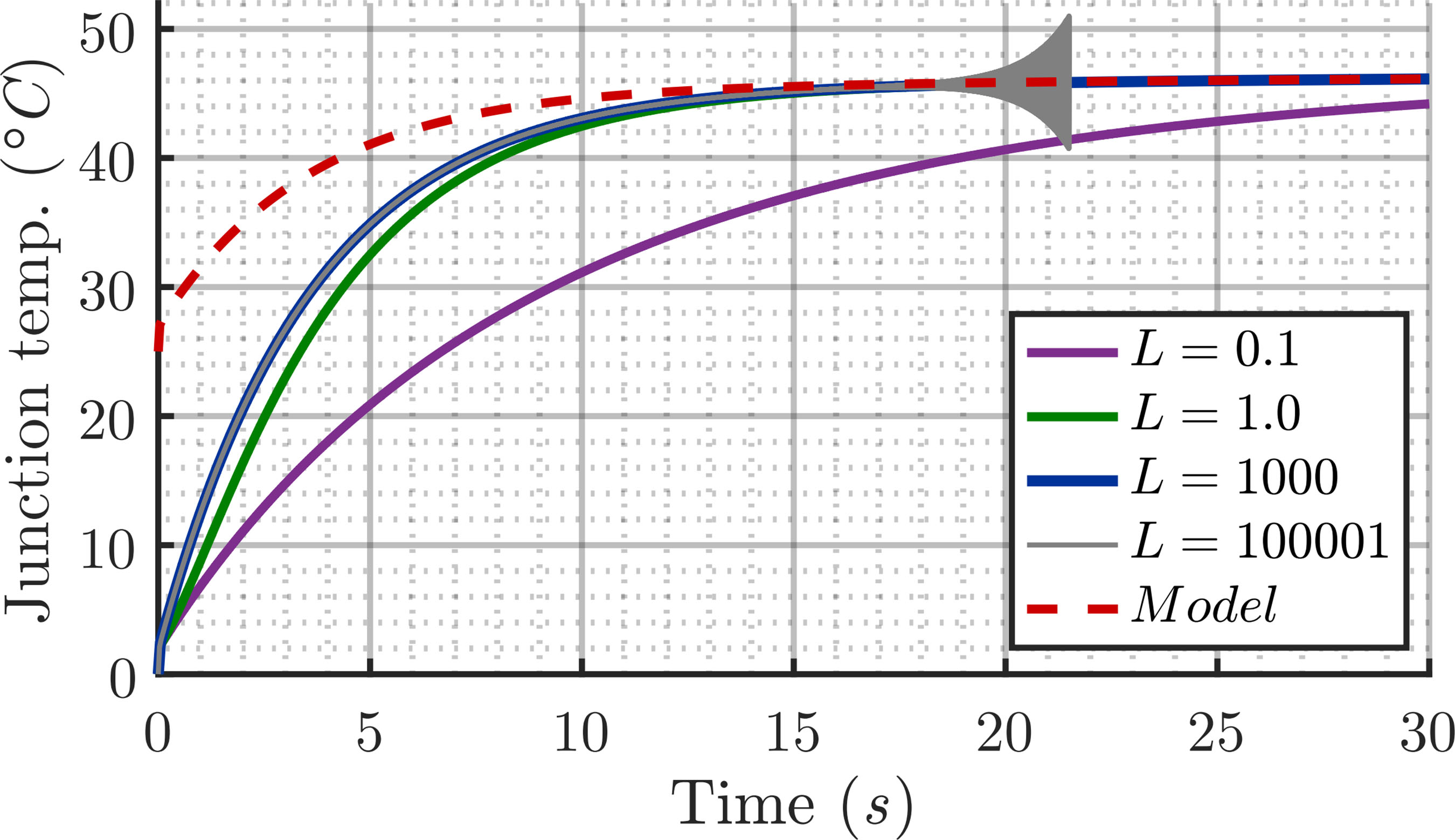
A simulation is carried out to validate the proposed observer structure. It is assumed that the losses of switches S1 and S2 (vide Figure 8) are constant at 10 W, and all initial temperature states are 25°C. In contrast, the observer initially states set to zero. Figure 7 shows the junction temperature in dashed red. It can be observed that the temperature increases from 25°C to 45°C for the simulated conditions. In addition, the impact of the Luenberger observer gain was evaluated. The results show that the gain selection directly affects the convergence dynamics of the observer. For very small gains, such as L = 0.1, the observer dynamic is slow. For very high gains, such as L = 100001, may lead to instability of the observer. From Figure 7 it is possible to conclude that a gain of L = 1000 provides a suitable dynamic response. Therefore, the gain vector was defined as:
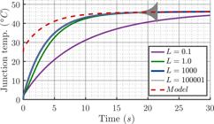
This gain vector proved to be adequate to ensure a fast observer response under current variations, while preserving the thermal hierarchy between junction and heatsink. Such a configuration guarantees that the estimated dynamics consistently follow the plant thermal behavior, which is essential for the stability and effectiveness of the estimation algorithm.
B. Experimental results
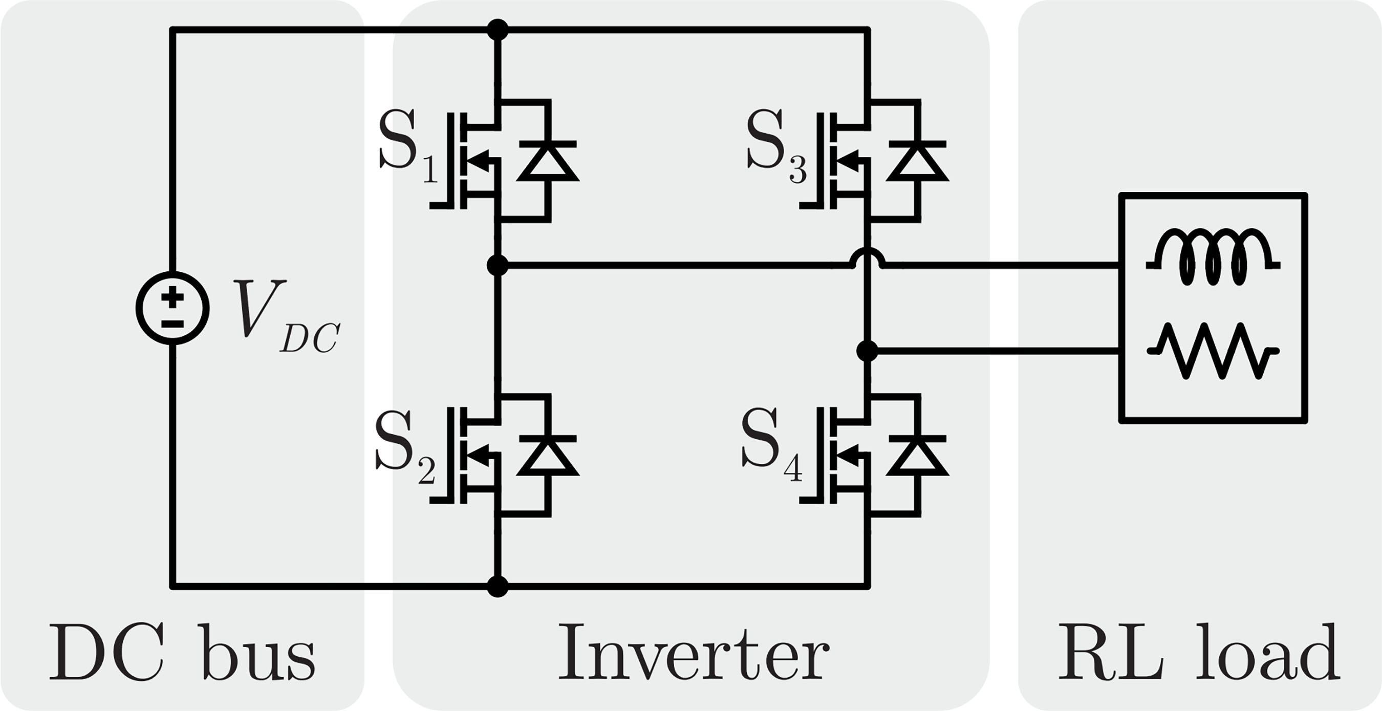
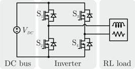
Experimental results were carried out to evaluate the proposed temperature observer. To achieve this, a setup composed by a power PCB, micro controller interface circuit and temperature acquisition was developed. The power board was designed to accommodate two SiC MOSFET MSCSM70AM10CT3AG half-bridge power modules connected to an RL load and the current is measured with an LEM LF 210-S current sensor. The thermal monitoring of heatsink is achieved using NTC sensors model NTCALUG01A103F. Figure 8 presents the setup schematic.
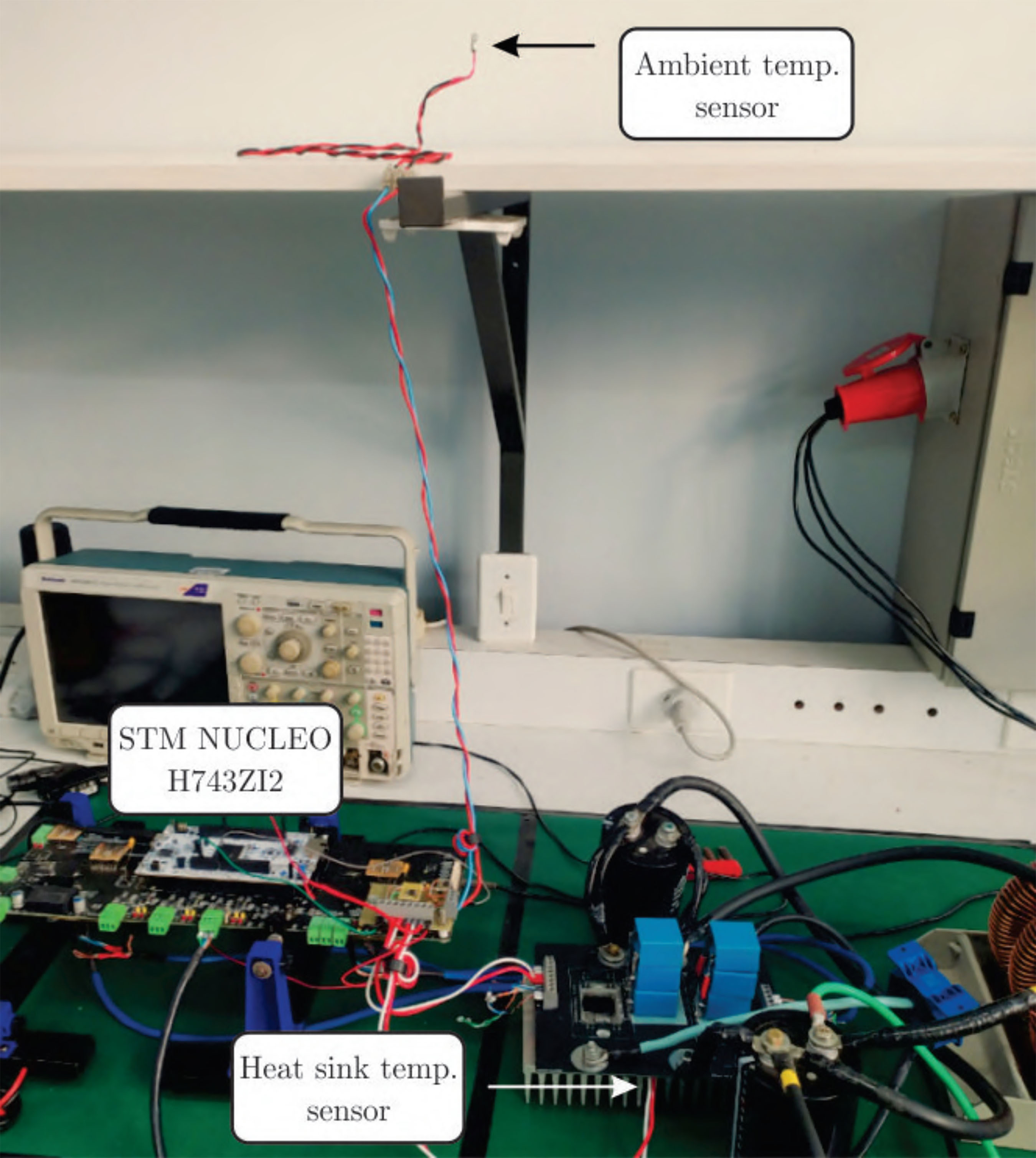
The inverter structure also clarifies the switching states referenced in the subsequent waveforms and thermal measurements. In this setup, the load current is regulated in closed loop using proportional–integral (PI) controllers, and all monitoring and control-law implementation are performed on an STM NUCLEOH743ZI2 microcontroller. Figure 9 presents the experimental setup and Table 1 presents the setup parameters.
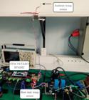
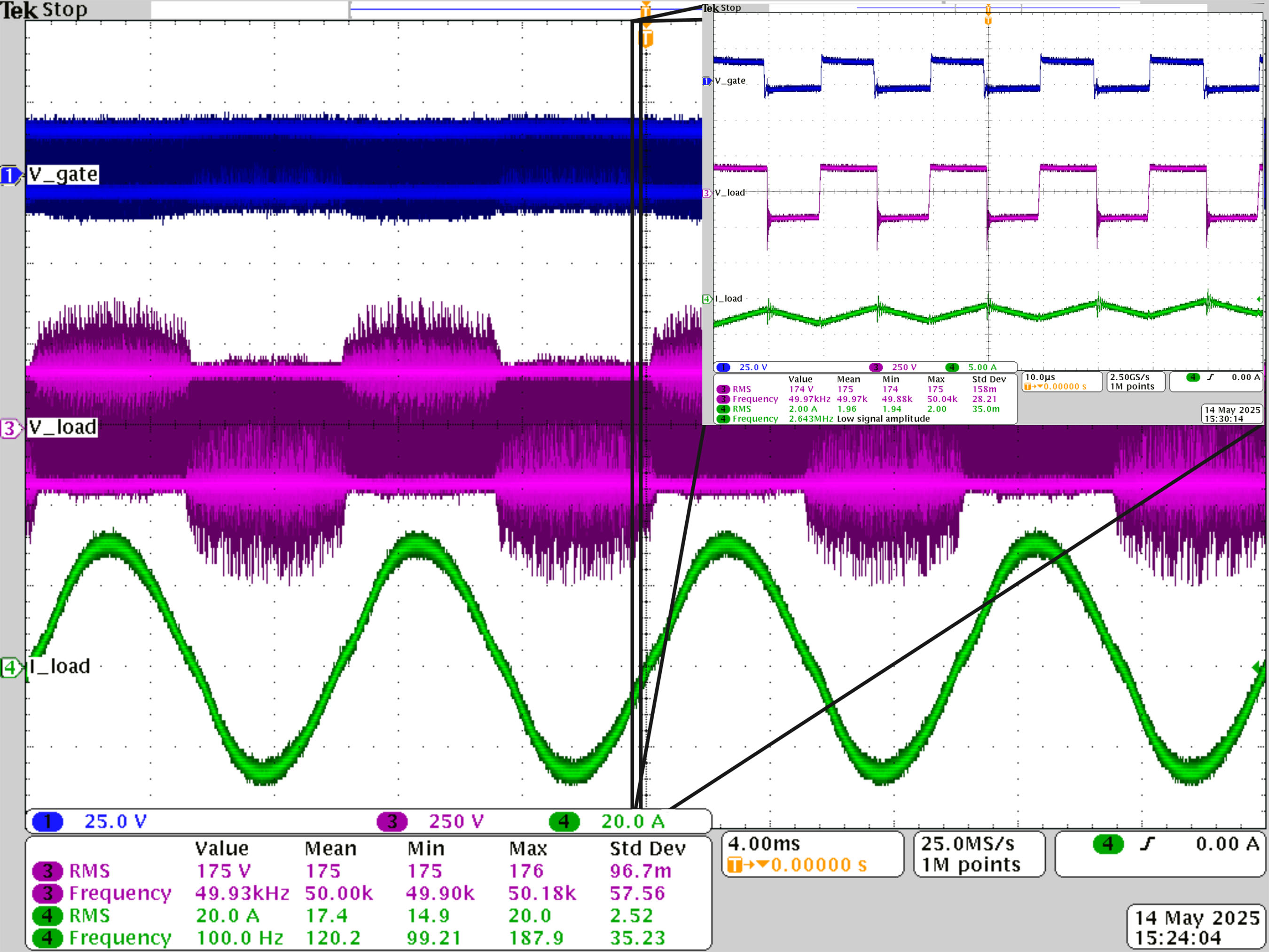
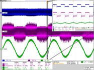
Figure 10 shows the waveforms measured during closed-loop operation, including the gate command signal, the load voltage, and the resulting load current. The load voltage exhibits the expected pulse-width modulated behavior, while the load current presents a smooth sinusoidal waveform, confirming proper current regulation by the control loop. The zoomed-in view highlights the switching transitions in greater detail, showing the synchronization between the rising and falling edges of the gate signals and the corresponding variations in voltage and current. This synchronization directly influences the switching losses responsible for heating the semiconductor junctions, making this information crucial for interpreting the temperature.
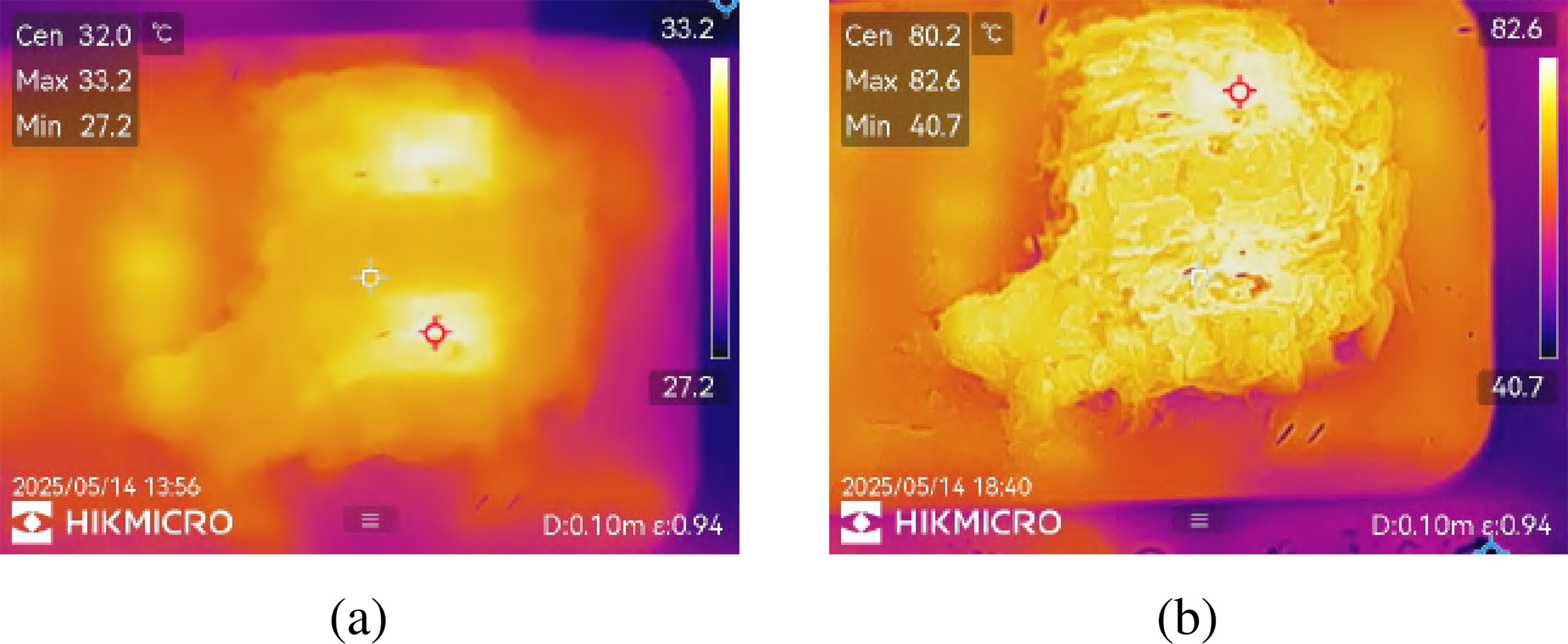
To validate the proposed junction temperature estimation technique, the casing of one power module was removed to allow direct access to the junction connection region. In this area, the encapsulation resin was removed exclusively around the area of interest on the device, enabling experimental verification of the junction temperature. Following this step, a high-emissivity coating was applied to the exposed junction region, allowing thermal data to be captured through infrared imaging using an HIKMICRO G31 camera. A load step was then applied to the full-bridge inverter connected to the RL load. Figures 11 (a) and 11 (b) illustrate the thermal images at the beginning and end of the experiment, highlighting the increase in temperature in the active region of the module, which is the main heat source of the system.
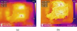
Thermal images at the junction region: (a) in the beginning (Time = 100 s) and (b) ending of the operation (Time = 16,5×10³ s).
The thermal images illustrate the temperature evolution at the junction region throughout the test. At the beginning of the operation (100 s, vide Figure 11 (a) ), the temperature distribution is moderate and relatively uniform. By the end of the test (16.5 × 10³ s, vide Figure 11 (b)), a significant temperature rise is observed in the central area, indicating the thermal regime established during prolonged operation. Furthermore, the localized temperature increase confirms that the removal of the gel in the region of interest was successful, allowing the actual heating of the device to be clearly visualized.
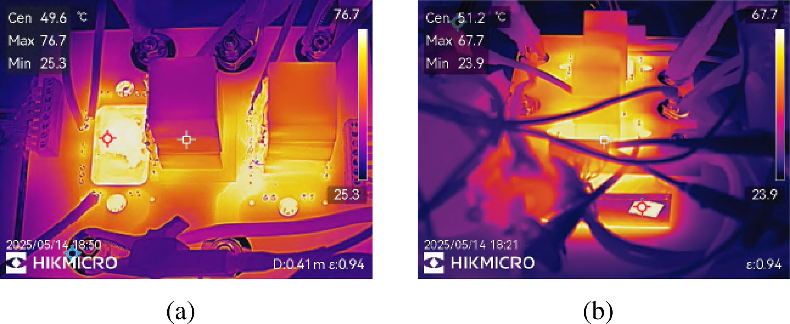
In addition to the junction region, the thermal distribution of the power PCB and the heatsink was also monitored, reinforcing the correlation between the physical sensors and the calculated values. These results are presented in Figures 12 (a) and (b).

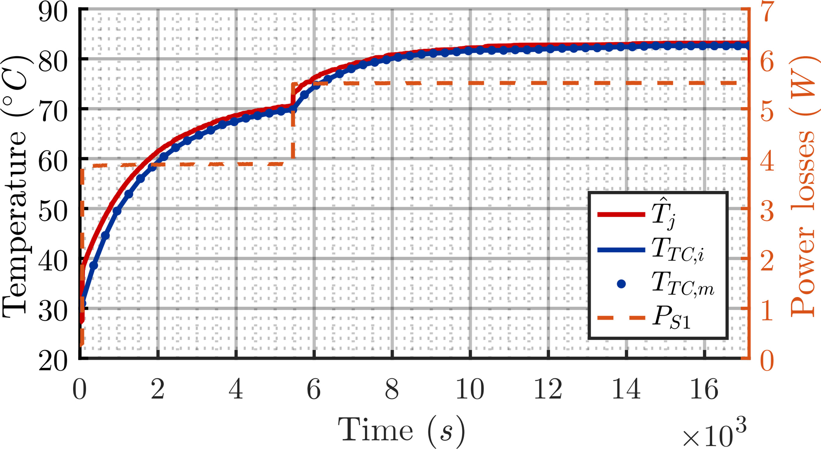
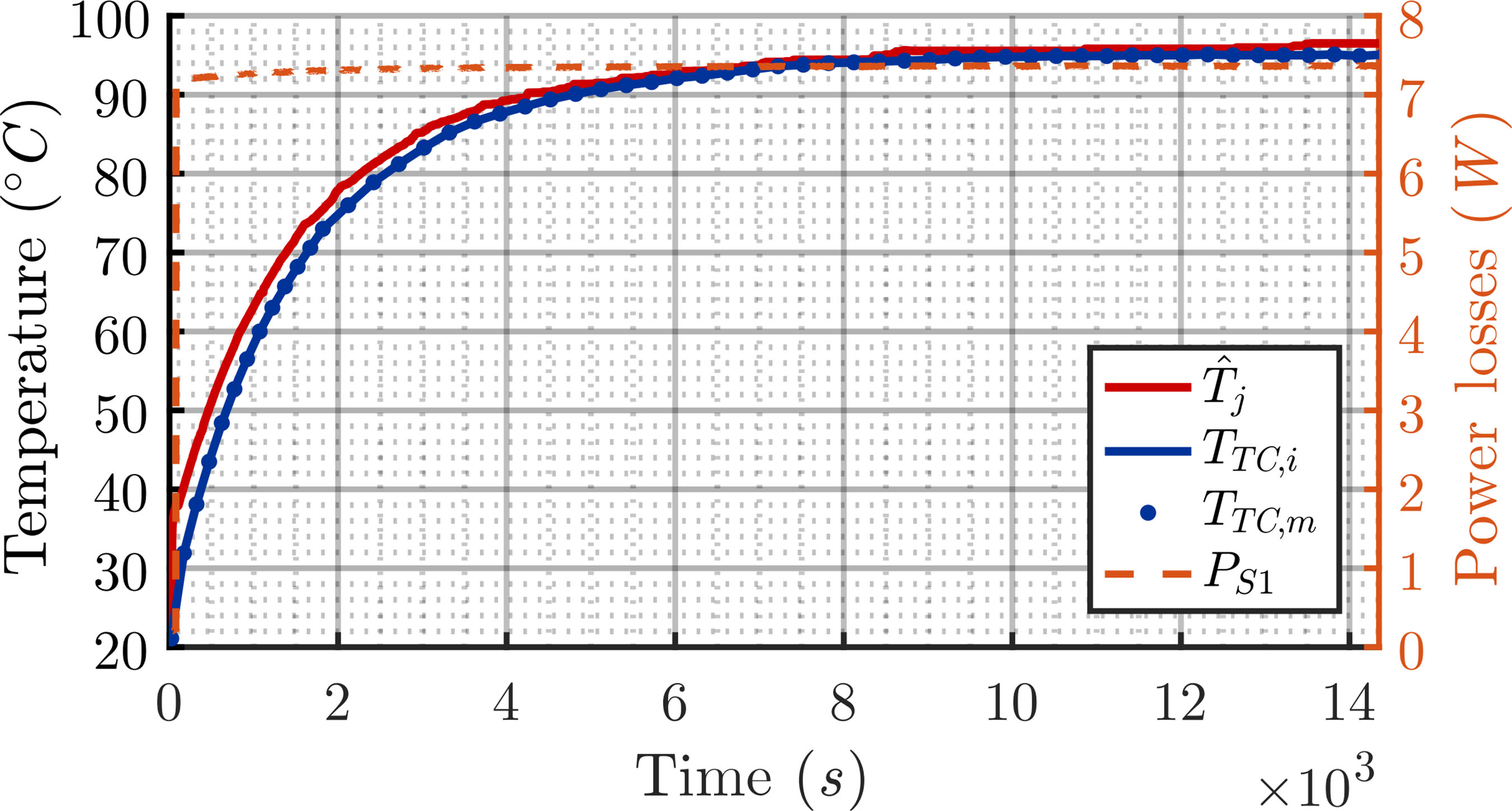
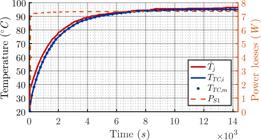
The first experiment applied a step load profile, starting at 15 Arms until 5500 s and then increasing to 20 Arms. Figure 13 compares the estimated junction temperature with thermal camera measurements, using PS1, which represents the system power losses obtained through experimental measurements, as well as the interpolated case temperature TTC,i, the measured case temperature TTC,m, and the estimated junction temperature Tˆj. In this context, TTC,i and TTC,m represent case temperature values that are very close to the junction temperature, due to the adopted measurement methodology. The results show a good correlation between the estimated and measured values, demonstrating that the observer can accurately reproduce the thermal dynamics of the junction. This agreement is particularly relevant during the load transition, when the temperature of the power devices increases significantly. The observer’s ability to capture this transient behavior reinforces its potential as an effective alternative to direct temperature sensing.

Comparison between the estimated temperature and the measured temperature via thermal camera.
To further evaluate the estimator’s robustness, a second experiment was conducted in which the load current was directly increased from 0 to 25 Arms, emulating a start-up condition with sudden power demand. The thermal response, shown in Figure 14 presents the system response to a load step applied to the converter, illustrating the corresponding thermal behavior of the power devices. The figure compares the junction temperature estimated by the observer with the case temperature obtained from thermal camera measurements and the interpolated temperature profile. The results show that the observer promptly follows the temperature rise induced by the load step, while maintaining close agreement with the measured and interpolated values. This close correspondence indicates that the proposed strategy can accurately capture the thermal dynamics of the system during load transients, including abrupt operating conditions.
Comparison between the estimated junction temperature and the measured temperature via thermal camera for a step of 25 Arms.
Using this methodology, it is possible to monitor and verify the thermal behavior of power devices. It can be applied in traction inverters, especially to prevent inverter burnout, as well as to serve as protection mechanisms and trigger alarms. Moreover, it provides a foundation for advanced functionalities such as active thermal protection, dynamic loss balancing, and optimized use of the thermal margin in power electronics systems. Its applicability to multiphase topologies or varying load profiles further expands its potential in modern power electronics, where reliability and efficiency are critical.
V. CONCLUSION
This work presented the modeling, implementation, and validation of a junction temperature estimation method for SiC Mosfets applied to traction inverters. Motivated by the increasing demand for sustainable mobility and the challenges associated with thermal management in high-power converters, a Luenberger state observer was developed to estimate the junction temperature based on a reduced-order thermal model. The approach relies on accessible variables such as ambient temperature, heat sink temperature, and calculated power losses, avoiding the need for invasive or costly measurement techniques. The proposed methodology was validated through both simulations and experimental assessments on a single-phase full-bridge inverter. Thermal images and physical sensors were employed to compare the estimated values with measured data. The results demonstrated a strong correlation, highlighting the accuracy of the observer in reproducing the thermal dynamics of the junction. In addition, the technique showed superior performance compared to the built-in module sensor, especially in capturing fast transients and abrupt load variations.
These findings confirm the robustness and practical applicability of the proposed observer for embedded thermal monitoring in power converters. Beyond improving system safety, the approach can also enable advanced functionalities, such as active thermal protection, dynamic loss balancing, and optimized use of the thermal margin of semiconductor devices. Future developments may extend this strategy to multiphase topologies and different cooling conditions, consolidating its potential as a versatile tool for future traction inverters.
ACKNOWLEDGMENT
This work was supported by Coordenação de Aperfeiçoamento de Pessoal de Nível Superior - Brasil (CAPES/PROEX) - Finance Code 001. The authors would also like to thank the Fundação de Desenvolvimento da Pesquisa - Fundep Mover/Linha V 27192.03.01/2022.04-00, and CNPq 305211/2025-0.
-
PLAGIARISM POLICY
This article was submitted to the similarity system provided by Crossref and powered by iThenticate – Similarity Check.
DATA AVAILABILITY
The data used in this research is available in the body of the document.
REFERENCES
-
1 C. Shi, Y. Tang, A. Khaligh, “A Three-Phase Integrated Onboard Charger for Plug-In Electric Vehicles”, IEEE Transactions on Power Electronics, vol. 33, no. 6, pp. 4716–4725, 2018, doi:10.1109/TPEL.2017.2727398.
» https://doi.org/10.1109/TPEL.2017.2727398 -
2 A. Griffo, J. Wang, K. Colombage, T. Kamel, “Real-Time Measurement of Temperature Sensitive Electrical Parameters in SiC Power MOSFETs”, IEEE Transactions on Industrial Electronics, vol. 65, no. 3, pp. 2663–2671, 2018, doi:10.1109/TIE.2017.2739687.
» https://doi.org/10.1109/TIE.2017.2739687 -
3 E. Zeyen, S. Kalweit, M. Victoria, T. Brown, “Shifting burdens: how delayed decarbonisation of road transport affects other sectoral emission reductions”, Environmental Research Letters, vol. 20, no. 4, p. 044044, mar 2025, doi:10.1088/17489326/adc290.
» https://doi.org/10.1088/17489326/adc290 -
4 M. Andresen, M. Schloh, G. Buticchi, M. Liserre, “Computational Light Junction Temperature Estimator for Active Thermal Control”, in 2016 IEEE Energy Conversion Congress and Exposition (ECCE), pp. 1–7, 2016, doi:10.1109/ECCE.2016.7854953.
» https://doi.org/10.1109/ECCE.2016.7854953 -
5 M. H. M. Sathik, J. Pou, S. Prasanth, V. Muthu, R. Simanjorang, A. K. Gupta, “Comparison of IGBT Junction Temperature Measurement and Estimation Methods-A Review”, in 2017 Asian Conference on Energy, Power and Transportation Electrification (ACEPT), pp. 1–8, 2017, doi:10.1109/ACEPT.2017.8168600.
» https://doi.org/10.1109/ACEPT.2017.8168600 -
6 N. Baker, L. Dupont, S. M. Beczkowski, F. Iannuzzo, “Proof-of-Concept for an On-Chip Kelvin-Emitter RTD Sensor for Junction Temperature Monitoring of IGBTs”, IEEE Transactions on Components, Packaging and Manufacturing Technology, vol. 14, no. 12, pp. 2240–2247, 2024, doi:10.1109/TCPMT.2024.3370951.
» https://doi.org/10.1109/TCPMT.2024.3370951 -
7 X. Dong, A. Griffo, D. Hewitt, J. Wang, “Reduced-Order Thermal Observer for Power Modules Temperature Estimation”, IEEE Transactions on Industrial Electronics, vol. 67, no. 12, pp. 10085–10094, 2020, doi:10.1109/TIE.2019.2959483.
» https://doi.org/10.1109/TIE.2019.2959483 -
8 T. N. Kabwangala, J.-P. Fradin, Y. Ariba, A. Marie, F. Gouaisbaut, “Observer based junction temperature estimation: 3D simulations and experimentations”, in 2023 29th International Workshop on Thermal Investigations of ICs and Systems (THERMINIC), pp. 1–6, 2023, doi:10.1109/THERMINIC60375.2023.10325885.
» https://doi.org/10.1109/THERMINIC60375.2023.10325885 -
9 X. Wang, A. Castellazzi, P. Zanchetta, “Full-Order Observer Based IGBT Temperature Online Estimation”, in IECON 2014 - 40th Annual Conference of the IEEE Industrial Electronics Society, pp. 1494–1498, 2014, doi:10.1109/IECON.2014.7048699.
» https://doi.org/10.1109/IECON.2014.7048699 -
10 F. Gao, B. Bilgin, J. Bauman, “Junction Temperature Estimation Based on Updating RC Network for Different Liquid Cooling Conditions”, in 2019 IEEE Transportation Electrification Conference and Expo (ITEC), pp. 1–6, 2019, doi:10.1109/ITEC.2019.8790576.
» https://doi.org/10.1109/ITEC.2019.8790576 -
11 M. Schumann, S. Ebersberger, K. Graichen, “Dynamic and Stationary State Estimation of Fluid Cooled ThreePhase Inverters”, in 2022 International Symposium on Power Electronics, Electrical Drives, Automation and Motion (SPEEDAM), pp. 171–178, 2022, doi:10.1109/SPEEDAM53979.2022.9842247.
» https://doi.org/10.1109/SPEEDAM53979.2022.9842247 -
12 M. Warwel, G. Wittler, M. Hirsch, H.-C. Reuss, “Real-Time Thermal Monitoring of Power Semiconductors in Power Electronics using Linear Parameter-Varying Nodels for Variable Coolant Flow Situations”, in 2014 IEEE 15th Workshop on Control and Modeling for Power Electronics (COMPEL), pp. 1–6, 2014, doi:10.1109/COMPEL.2014.6877142.
» https://doi.org/10.1109/COMPEL.2014.6877142 -
13 K. Kumar, M. Bertoluzzo, G. Buja, F. Ortenzi, “Quantitative Analysis of Efficiency Improvement of a Propulsion Drive by Using SiC Devices: A Case of Study”, Advances in Power Electronics, vol. 2017, pp. 1–10, 02 2017, doi:10.1155/2017/9149472.
» https://doi.org/10.1155/2017/9149472 -
14 Y. Dong, L. Che, Z. Fan, Q. Zou, G. Lei, “Effects of OnState Resistance Temperature Effect on The Static Current Balancing Capability of SiC MOSFET Power Module”, in 2022 23rd International Conference on Electronic Packaging Technology (ICEPT), pp. 1–6, 2022, doi:10.1109/ICEPT56209.2022.9872596.
» https://doi.org/10.1109/ICEPT56209.2022.9872596 -
15 Z. J. Shen, Y. Xiong, X. Cheng, Y. Fu, P. Kumar, “Power MOSFET Switching Loss Analysis: A New Insight”, in Conference Record of the 2006 IEEE Industry Applications Conference Forty-First IAS Annual Meeting, vol. 3, pp. 1438–1442, 2006, doi:10.1109/IAS.2006.256719.
» https://doi.org/10.1109/IAS.2006.256719 -
16 E. O. Prado, P. C. Bolsi, H. C. Sartori, J. R. Pinheiro, “Simple analytical model for accurate switching loss calculation in power MOSFETs using non-linearities of Miller capacitance”, IET Power Electronics, vol. 15, no. 7, pp. 594–604, 2022, doi:10.1049/pel2.12252.
» https://doi.org/10.1049/pel2.12252 -
17 P. H. A. S. e. Silva, L. A. B. Viera, R. Camponogara, H. Pinheiro, R. P. Vieira, “Analysis of the Impact of Semiconductor Losses in High-Density Power Inverters”, in 2023 IEEE 8th Southern Power Electronics Conference and 17th Brazilian Power Electronics Conference (SPEC/COBEP), pp. 1–6, 2023, doi:10.1109/SPEC56436.2023.10407626.
» https://doi.org/10.1109/SPEC56436.2023.10407626 -
18 Microsemi Corporation, MSCSM70AM10CT3AG Datasheet: Phase Leg SiC MOSFET Power Module , Microchip Technology Inc., apr 2020, URL: https: //ww1.microchip.com/downloads/aemDocuments/ documents/PPM/ProductDocuments/DataSheets/ Microsemi_MSCSM70AM10CT3AG_Phase_Leg_SiC_
» https: //ww1.microchip.com/downloads/aemDocuments/ documents/PPM/ProductDocuments/DataSheets/ Microsemi_MSCSM70AM10CT3AG_Phase_Leg_SiC_
Edited by
-
Associate Editor
Renata O. de Sousa https://orcid.org/0000-0002-9556-5260
-
Editor-in-Chief
Allan F. Cupertino https://orcid.org/0000-0001-8418-1985
History
-
Received
15 Sept 2025 -
Reviewed
15 Dec 2025 -
Reviewed
30 Dec 2025 -
Accepted
20 Jan 2026 -
Published
05 Feb 2026