 Impact of Substrate and Additive on the As-Prepared Bi2-xSbxTe3 Thermoelectric Film by Electrodeposition
Abstract
In order to investigate the influence of substrate and additive on Bi2-xSbxTe3 thermoelectric films, Bi2-xSbxTe3 films were successfully fabricated on the surface of indium-tin-oxide (ITO) and stainless steel (SS) in HNO3 solution using constant potential technique. Meanwhile, Bi2-xSbxTe3 film was prepared on ITO substrate using the electrolyte containing thiourea as an additive. The phases of the annealed thin films were determined by X-ray diffraction (XRD). Besides, the morphologies of the annealed films were characterized by scanning electron microscopy (SEM), and the property parameters of Bi2-xSbxTe3 thermoelectric films were also tested. The results showed that the as fabricated thin films on ITO in electrolyte with or without thiourea and SS substrates were pure (Bi0.5Sb0.5)4Te3. Moreover, the films prepared on ITO or SS substrate had a granular structure, but the surface morphologies were quite different. The (Bi0.5Sb0.5)4Te3 film electrodeposited on ITO in electrolyte without additive presented walnut seed-like morphology, while the annealed film electrodeposited in electrolyte with additive presented rose-like morphology. However, the (Bi0.5Sb0.5)4Te3 film electrodeposited on SS presented cotton-like morphology. In addition, the annealed film electrodeposited on ITO in electrode with additive was denser; thereby, it has the highest electrical conductivity of 984.50 S cm-1 compared with the other two films.
Keywords:
substrate; additive; thermoelectric; Bi2-xSbxTe3 film; phase; morphology
Introduction
Advanced energy materials represented by thermoelectric (TE) materials are one of the new materials urgently needed for the development of emerging industries. TE material is an energy conversion material, which uses the Seebeck effect and Peltier effect of semiconductor materials to realize the mutual conversion between heat energy and electric energy.1 It is an environmentally friendly energy conversion material, which is mainly used in TE power generation and TE refrigeration.2 However, so far, the progress of TE power generation is slow, and it has only been applied in a few occasions and not commercialized.3 Although TE refrigeration has been commercialized for decades, it is only limited to the application of small power refrigeration.4 As for the application of high-power TE refrigeration system, it is technically feasible but economically unfeasible.5 This is mainly due to the low TE performance of currently discovered TE materials.4 Good TE materials must have a large Seebeck coefficient (α), a small thermal conductivity (λ), and a high electrical conductivity (σ).6 These requirements can be described by the TE figure of merit (Z), defined as Z = α2σ/λ.7 Because each TE material has its own suitable working temperature range, it is customary to use ZT (T is absolutely temperature) to describe the TE performance of material. The calculation of the most basic TE power generation or refrigeration circuit shows that both for power generation and refrigeration, the higher the ZT value of TE material, the better. To surpass other traditional refrigeration or power generation technologies, ZT needs to reach more than 4 and 2, respectively.4,8 At the same time, the three parameters associated with Z are not independent. They are all functions of the density of free electrons (and holes). Roughly speaking, σ is proportional to the carrier concentration (n) according to σ = neμ, where e is the charge on the electron, and μ is the carrier mobility;9 α decreases with the increase of n; λ is the sum of phonon thermal conductivity and electron thermal conductivity: λ = λs + λe, where λs is independent of n, and λe is proportional to n. α, σ and λ of TE materials are all functions of n. The three parameters are not independent of each other, but coupled and restricted to each other.10,11
In recent years, with the progress of technology, many researchers have tried to decouple the mutual constraints between α, σ and λ in order to obtain higher value of ZT.12 Up to now, the main strategies that can enhance the ZT are as follows: (i) nano engineering. In the early 1990s, a team of Prof Mildred S. Dresselhaus pointed out that materials with nanostructures might have good TE effects based on the principles of quantum mechanics and the development of nanotechnology.9 Dresselhaus et al.9 suggested that the TE material should be prepared into nanofilms, nanowires, nanotubes, etc., so that the TE performance will be greatly improved; (ii) interface engineering: in the TE field, phase interface engineering can improve the TE performance of materials because interfacial scattering can reduce lattice thermal conductivity and energy filtering can enhance the effective mass of density of state (DOS).13 Wu et al.14 designed the interface of Cu2MgFe/Mg2Sn0.75Ge0.25, and the single-leg TE device based on this material achieved a high-power density of 2.6 W cm-2 at 370 ºC and a maximum conversion efficiency of 8%. Compared to other Mg2(Si,Ge,Sn)-based TE devices, this is already a record-breaking value. (iii) Entropy engineering: the high disorder in atomic distribution caused by increased entropy can introduce intense lattice distortion in materials, thereby altering the phonon transport paths of solid materials and reducing their lattice thermal conductivity.15 Therefore, based on the electrical and thermal transport behaviors of TE materials, the concept of high entropy may become a new strategy for effectively optimizing the performance of TE materials.15 In addition, chemical fluctuations are ubiquitous in high-entropy materials and play a significant role in TE field. Shi and co-workers16 designed and synthesized a series of samples with ultra-high configurational entropy. These fluctuations, coupled with unusual atomic occupancy, resulted in abnormally low lattice thermal conductivity.16 Combining optimized carrier concentration and maintaining good carrier mobility, a high ZT value of 1.2 was achieved at 750 K, surpassing most previously reported AB2Sb2-type Zintls.15 He and co-workers17 had developed a high-performance PbSe-based high-entropy alloy TE material based on entropy-driven structural stability effect and fabricated an efficient TE power generation device. This work effectively guided the application of high-entropy concepts in the development of high-performance TE materials. Moshwan et al.15 extensively studied the effectiveness of entropy engineering in compounds, and pointed out the status and challenges of entropy engineering in the TE field. In addition, Liu and co-workers18 made a major breakthrough in ionic room temperature TE materials. Through the synergistic effect of ion diffusion entropy and reaction entropy of redox pair, a huge TE potential effect of 17 mV K-1 was achieved in quasi-solid ionic gels. (iv) Defect engineering: is an effective strategy for regulating the performance of TE materials and has great potential for improving the performance of TE materials.19 Wu et al.19 summarized the latest progress of defect engineering in enhancing the performance of TE materials and discussed how defect engineering could boost the performance of TE materials. Qiu et al.20 achieved excellent TE performance by introducing high-density line defects into Bi0.4Sb1.6Te3.72 material. This work proposed an effective strategy for the synergistic optimization of texture, TE property and mechanical strength in Bi2Te3-based materials. (v) Doping strategy: can increase the disorder of materials, thereby enhancing their entropy. Wang and co-workers 21 doped Bi2Te3 and prepared Bi0.5Sb1.5Te3 film using electrochemical deposition in nitric acid solution. In addition, Kim et al.22 doped Bi2Te3 and prepared Bi2Te3-xSex film by a pulsed electrodeposition method that simultaneously regulated current and potential. Performance tests showed that the power factor of the prepared film (with a maximum value of 1920 mW m-1 K-2) was significantly higher than that of the Bi2Te3-xSex film prepared using constant potential deposition technology. This was attributed to the acceptor doping of Se can increase n in the film, and the increased hole mobility leads to an improvement in the σ of the TE material, thereby enhancing its TE performance. (vi) Other strategies. In view of the optimization of μ, Qin and Zhao23 proposed a “grid” strategy based on component-procedure regulation to obtain higher mobility by regulating the intrinsic defects of materials.
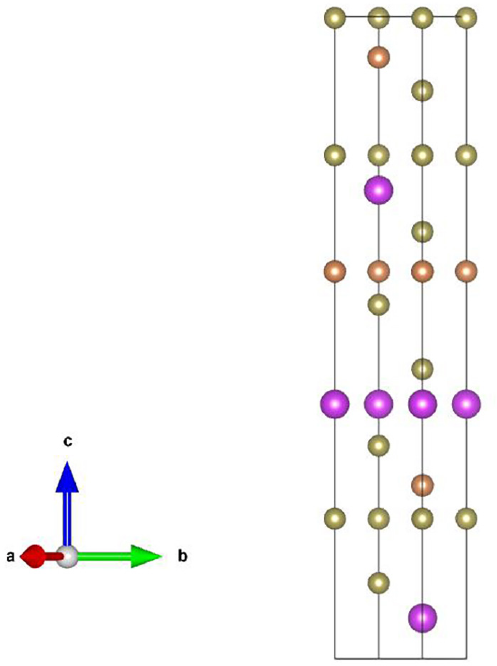
After decades of efforts, Bi2Te3 alloy is still the state-of-the-art TE refrigeration material with excellent TE property near room temperature.2,24 This is ascribed to compounds composed of heavy elements are typically used due to the relatively small frequency range of phonons and their low group velocity in phonon transport. Bi2Te3 is a compound containing the heavy metal element Bi.25 At the same time, due to the presence of lone pairs of electrons and resonance bonds, this compound exhibits strong non-harmonicity, further hindering heat transfer.25 However, the extremely low abundance of the Te element in Bi2Te3 has led to a severe shortage of TE cooling devices. Additionally, this material suffers from poor processability, low yield and high-power consumption during device operation. Furthermore, two-dimensional materials exhibit unique advantages in the fields of electronics, optics and quantum information due to their low dimensionality, strong correlation and topological effects. Thus, doping strategy was adopted to dope Bi2Te3 and prepared Bi2-xSbxTe3 ternary films. To our best knowledge, there was little work about investigating the effects of substrates and additives on the phase and morphology of Bi2-xSbxTe3 film. In our work, indium-tin-oxide (ITO) and stainless steel (SS) were used as substrates, and thiourea was used as an additive to prepare Bi2-xSbxTe3 films. The crystal structure of Bi2-xSbxTe3 is shown in Figure 1.
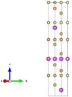
Crystal structure of Bi2-xSbxTe3. The purple atoms are Bi, the brown atoms are Sb and the green atoms are Te.
To date, the methods for preparing films include molecular beam epitaxy,26 metal-organic chemical vapor deposition (MOCVD),27 atomic layer epitaxy,28 electrochemical deposition,2 and so on. Among these methods, electrochemical techniques offer numerous advantages: lower cost, fast deposition rate, easier control over film thickness, and even the ability to select the preparation of n-type or p-type film by controlling the deposition potential.29 Therefore, in our work, Bi2-xSbxTe3 TE ternary films were prepared by electrochemical deposition. And the effects of substrates and additive on phase, morphology as well as properties were systematically investigated.
Experimental
Materials and instruments
Bi(NO3)3•5H2O, TeO2, Sb2O3, C4H6O6, thiourea and HNO3 were of analytical reagent grade and bought from commercial corporation (Sinopharm Chemical Reagent Co., Ltd., China). They were used as-received without further purification. ITO and stainless steel SS (area 1 × 1 cm2) were purchased from Wuhu Changxin corporation. ITO or SS, Pt sheet (area 1 × 1 cm2) and SCE (saturated calomel electrode) were used as the working electrode, counter electrode and reference electrode, respectively. The electrochemical workstation (CHI760E, Shanghai Chenhua Company) was used to prepare the samples. Magnetic stirrer (DF-101S, Gongyi Yuhua Instrument Co., Ltd.) was used to stir the solution in order to make the solution become transparent.
Preparation of electrolyte and samples
0.1213 g Bi(NO3)3•5H2O and 0.2394 g TeO2 were precisely weighed and transferred into a little beaker containing 1 M HNO3 solution, followed by stirring until the solution became clear. Then, 0.2915 g Sb2O3 was weighed and transferred into the 50 mL beaker with 1 M HNO3 solution followed by stirring, and 1.5009 g C4H6O6 were accurately weighed and put into the beaker containing Sb2O3 followed by stirring until the solution became transparent. The function of tartaric acid was to dissolve Sb3+. Next, the two solutions were mixed and continuously stirred for about 5 min. Another solution was prepared at the same manner. Finally, 26 mg thiourea were accurately weighed and put into one of the mentioned above solutions in order to investigate the effect of additive on phase and morphology of the annealed film. Obviously, thiourea was used as a kind of additive. Then, two different electrolytes (2.5 mM Bi3+ + 10 mM Sb3+ + 15 mM Te4+ + 0.1 M HNO3 and 2.5 mM Bi3+ + 10 mM Sb3+ + 15 mM Te4+ + 0.1 M HNO3 + 26 mg thiourea) were ready for later use.
Prior to use, ITO and SS were cleaned with ethanol in an ultrasonic cleaner and washed by deionized water (homemade). After that, they were dried in the air at room temperature. Then, ternary films were deposited by potentiostatic mode in three-electrode system. The deposition time was fixed at 20 min. Then, three films were fabricated. The films that were electrodeposited on ITO and SS in the electrolyte without additive were named sample 1 and sample 2, respectively. The Bi2-xSbxTe3 film that was electrodeposited on ITO in the electrolyte containing additive was named sample 3. Next, samples 1, 2 and 3 were all annealed at 200 ºC for 3 h.
Material characterization
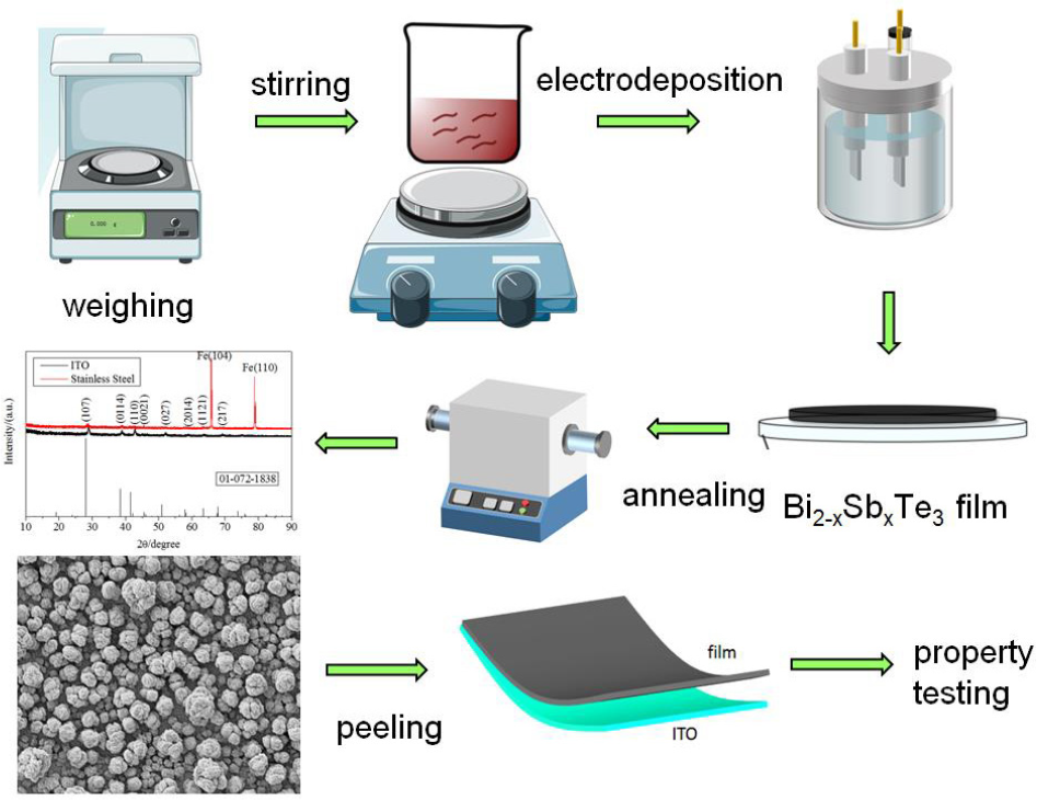
The crystal phase of the annealed films was characterized by X-ray diffraction (XRD, Bruker D8 Advance). The morphologies of the synthesized films were investigated by field emission scanning electron microscopy (FE SEM, JEOL JSM5510LV). The thickness of the annealed films was measured by alpha-step surface profiler (ET4000a, Kosaka). Carrier concentration (n), electrical conductivity (σ) and Hall mobility (μ) of the films were determined at room temperature using a Hall effect testing system (HMS 3000, Ecopia) with a magnetic field of 0.55 T. The α value was measured by the slope of the linear relationship between the thermal electromotive force and temperature difference (ca. 10 K) between the two ends of each film. Thermal electromotive force was measured by using two K-type NiCr-NiSi thermocouples attached to the two Cu bulks. The error of the determined α values was below 10%. The illustration of the experimental scheme for producing and characterization of Bi2-xSbxTe3 films is shown in Figure 2.
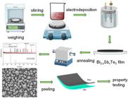
The illustration of the experimental scheme for producing and characterizing Bi2-xSbxTe3 films.
Results and Discussion
Studies of cyclic voltammetry
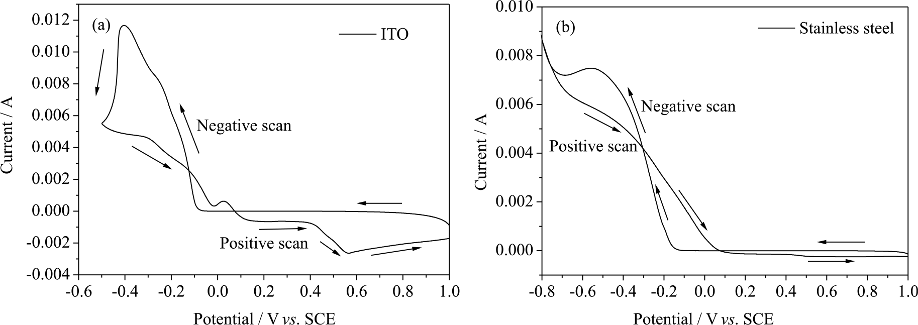
The study of cyclic voltammetry (CV) aims at investigating the redox reaction of the working electrode in certain electrolyte. Prior to electrodeposition, the deposition potential should be identified firstly by CV. As indicated in Figure 3, the CV curves of the different substrates were quite different. At the same time, it could be observed that whether ITO or SS was used as the substrate for CV testing, the resulting CV curves were asymmetrical, indicating that the electrochemical reaction was irreversible. In Figure 3a, during the negative sweep, a reduction peak appeared at -0.446 V, corresponding to the maximum reduction deposition rate of the ternary film Bi2-xSbxTe3. While in Figure 3b, during the negative scan, a reduction peak appeared at -0.553 V, corresponding to the maximum reduction rate of the ternary film Bi2-xSbxTe3. This indicated that depositing Bi2-xSbxTe3 on ITO was easier than on SS.
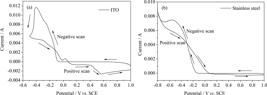
The CV curves of (a) ITO, (b) SS substrate in electrolyte consisted of 0.1 M HNO3 + 0.0025 M [Bi3+] + 0.0015 M [Te4+] + 0.002 M [Sb3+], the scan rate: 0.01 V s-1 and scan range: (a) -0.5-1 V, (b) -0.8-1 V.
Constant potential deposition
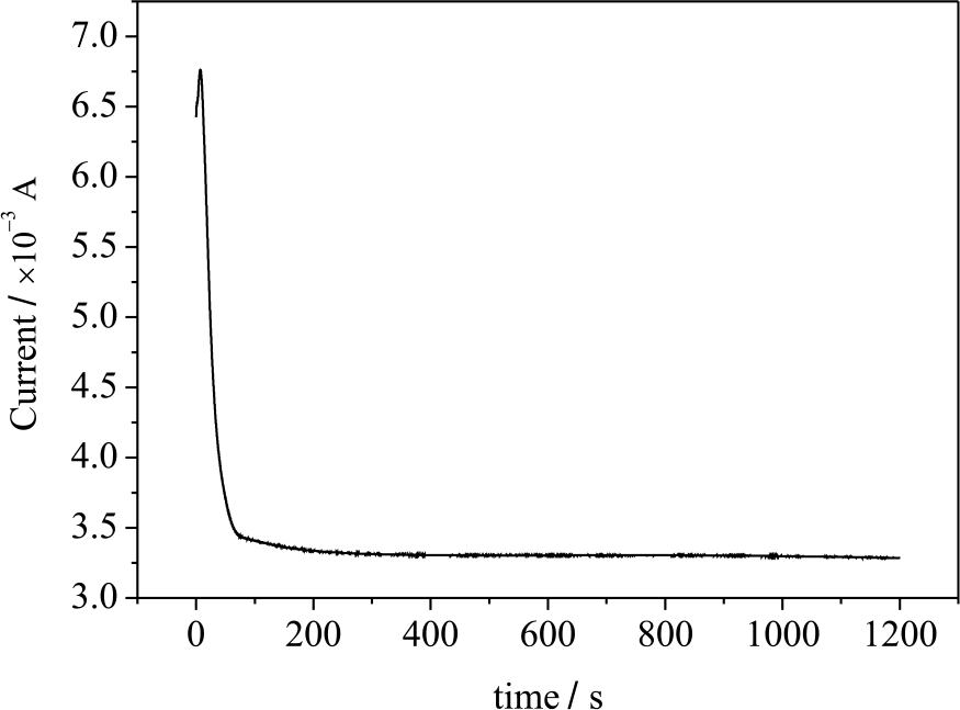
Because low potential deposition was good for the preparation of relative dense films, combined with the CV data in Figure 3, -0.1279 V was selected as the deposition potential for constant potential deposition, and the deposition time was 20 min to prepare the ternary film.
Figure 4 shows the potentiostatic deposition curve with ITO as the substrate. From the figure, it could be seen that at the very beginning of the potentiostatic deposition, the current dropped sharply. This was attributed to the rapid nucleation of Bi2-xSbxTe3 on the ITO electrode at the start of the potentiostatic deposition. Since Bi2-xSbxTe3 was a semiconductor material with poorer conductivity than ITO conductive glass, the resistance of the three-electrode system increases rapidly. Due to the constant potential, the current decreases rapidly. When the target atoms covered the surface of the working electrode with a layer (from the Figure 4, this time was approximately 60 s), the current basically stabilized. As shown in Figure 4, the current basically stabilized until the end of the electrodeposition after about 60 s.
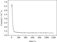
The potentiostatic electrodeposition curve with SS as the substrate was similar to that with ITO as the substrate.
XRD analysis
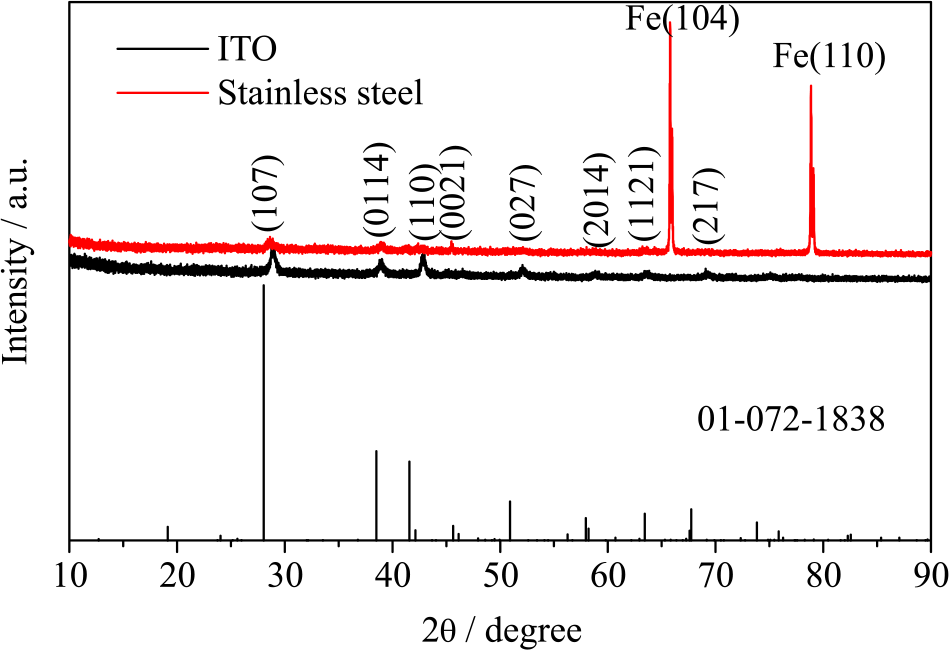
The film prepared by electrodeposition method required annealing to obtain a crystalline and preferentially oriented film.4 Meanwhile, since low-temperature annealing was beneficial for TE performance, high-temperature annealing could lead to grain size growth.15 Therefore, the electrochemically deposited films were firstly subjected to low-temperature annealing (200 ºC, 3 h) before XRD analysis, as shown in Figure 5.
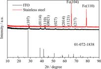
Figure 5 exhibits the XRD patterns of the annealed Bi2-xSbxTe3 in ITO and SS substrates. From Figure 5, we could see that the diffraction peaks in the XRD pattern of the samples electrodeposited on ITO and SS corresponded to the reported rhombohedral (Bi0.5Sb0.5)4Te3 (JCPDF card No. 01-072-1838). Additionally, from Figure 5, it could also be observed that the XRD pattern of the sample prepared on a SS substrate showed two distinct Fe diffraction peaks originated from the SS substrate, corresponding to the (104) and (110) crystal planes of the reported Fe (JCPDF card No. 00-050-1275). The remaining diffraction peaks could be indexed to the reported (Bi0.5Sb0.5)4Te3 (JCPDF card No. 01-072-1838). This indicated that pure (Bi0.5Sb0.5)4Te3 could be fabricated regardless of whether ITO or SS was used as the substrate.
Moreover, regardless of whether ITO or SS was used as the substrate, the diffraction peaks of the crystal planes (107), (0014), (110) and (027) all showed a slight rightward shift on Figure 5. According to Bragg’s law: 2d*sinθ = mw (m was on behalf of diffraction series, w was wavelength), when the wavelength remains constant, the variation in the diffraction angle 2θ directly reflects changes in the d value. The shifts of diffraction angles of the electrodeposited film occurred because residual stresses were introduced during electrodeposition or post-processing. These stresses induced elastic distortion in the lattice, altering the lattice constants and consequently modifying the d-value. Generally, tensile stress causes d-value increase. Thus, it shifts the 2θ angle toward smaller values. While compressive stress reduces d-value, it causes the 2θ angle to shift toward larger value. Therefore, the observed rightward shift in the diffraction angle was likely due to compressive stress generated during the electrodeposition or annealing process for the film. At the same time, in the XRD pattern of the electrodeposited film with SS as the substrate, the diffraction peaks from the substrate were so sharp that the intensity of the other diffraction peaks from the sample was lower compared to the diffraction peaks of the sample with ITO as the substrate. Furthermore, compared with the XRD pattern of the sample prepared with SS as the substrate, the diffraction peak of the (107) crystal plane in the XRD pattern of the sample deposited with ITO as the substrate showed a rightward shift. Additionally, by referring to the standard card, the sample deposited on ITO showed a preferred orientation in the (110) crystal plane, which was considered the optimal crystal orientation for obtaining excellent TE properties.1 Based on this, it was speculated that the thermoelectric property of the film prepared on ITO were superior to those of the film fabricated on SS substrate.
Analysis of surface morphology and forming mechanism
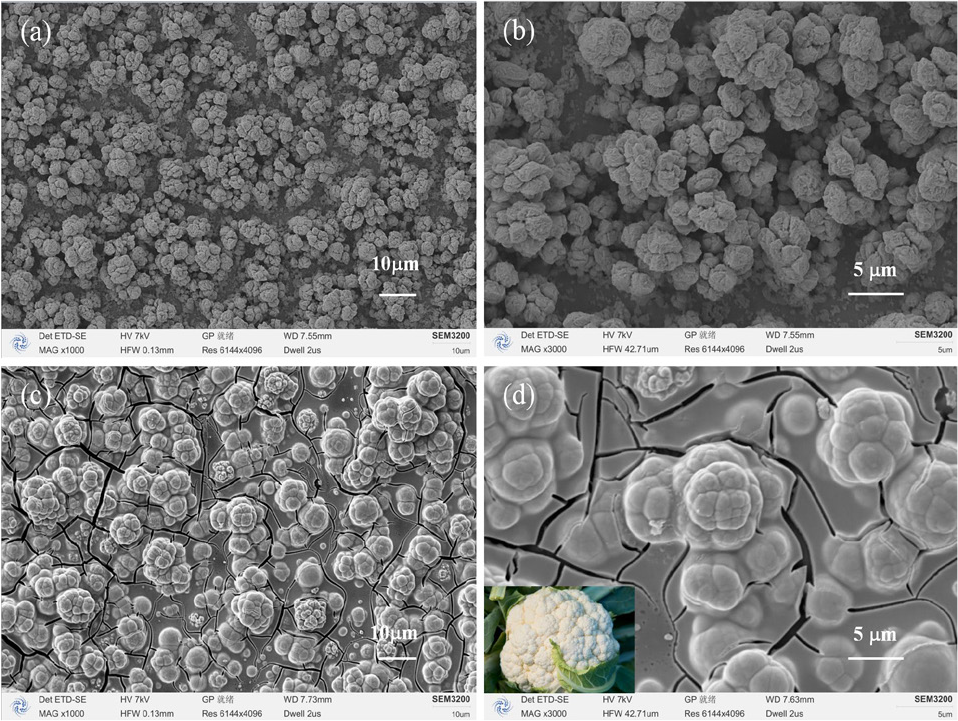
Figure 6 showed the SEM images of Bi2-xSbxTe3 films prepared on ITO and SS substrates by potentiostatic deposition mode. From the low-magnification images, regardless of whether the substrate was ITO or SS, the films surface exhibited a granular structure, with small particles aggregating to form larger particles of varying sizes. Figures 6a and 6b show SEM images of the film prepared on ITO substrate. From the high-magnification image, it could be observed that the surface of the prepared ternary film has a “walnut kernel”-like morphology. Figures 6c and 6d were SEM images of the ternary film prepared on SS substrate. As indicated from Figure 6d, the surface of the ternary film exhibited a cauliflower-like morphology. Additionally, it could be observed that the films prepared on both ITO and SS substrates were not dense enough in appearance.
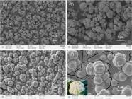
SEM images of Bi2-xSbxTe3 prepared on ITO (a) and (b), SS (c) and (d). The inset of (d) is a picture of cauliflower.
According to crystal growth theory, the formation of materials was a competitive process between nucleation and grain growth. If the nucleation rate was greater than the grain growth rate, more nuclei would form, the grains would be refined, and the resulting material would be more compact. Conversely, if the grain growth rate was greater than the nucleation rate, the material would tend to form a granular morphology. Furthermore, according to the theory of crystal solidification, the growth morphology during crystal solidification was not only related to the microstructure at the liquid-solid interface but also depended on the temperature distribution in the liquid phase at the front edge of the interface. Under a negative temperature gradient, the latent heat of crystallization generated at the phase boundary could be dissipated through both the solid and liquid phases. The shift of the phase interface was not solely controlled by the heat transfer rate of the solid phase. In such cases, if part of the phase interface protrudes into the preceding liquid phase, it can be in a cooler liquid phase, increasing the growth rate of the protruding part and further extending into the liquid. This allows for continued growth on the original particle. This is the possible mechanism for the formation of granular structures. That is under specific electrochemical preparation conditions in this work, whether ITO or SS was used as the substrate, the Bi2-xSbxTe3 film had a granular structure, which was caused by the grain growth rate being greater than the nucleation rate. This also led to the membrane microstructure being not dense enough.
Effect of additive on phase and morphology of Bi2-xSbxTe3 film
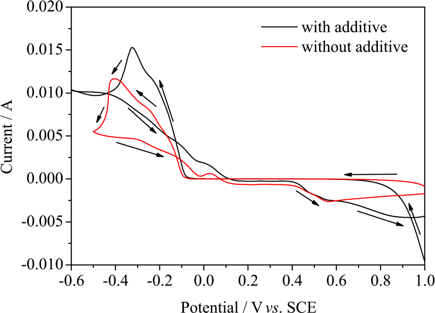
In order to study the effect of additive on the preparation of Bi2-xSbxTe3 film by electrodeposition, thiourea was used as an additive and other conditions were kept unchanged. Figure 7 shows the CV of ITO substrate with and without additive. From the graph, it could be seen that under the presence of additive, the reduction rate of Bi2-xSbxTe3 film reached its maximum at -0.3231 V. During the positive sweep, within the scanning range of -0.6 to 1 V, the oxidation reaction began at 0.4 V, with no significant oxidation peak. In the CV curve without additive, the reduction reaction started at -0.0605 V, with the reduction rate reaching its maximum at -0.4054 V. During the positive sweep, the oxidation reaction began around 0.3779 V, with the oxidation rate reaching its maximum at approximately 0.565 V. It was indicated that the additive had a significant effect on both reduction and oxidation reactions. In this electrochemical system, the additive shifted the reduction peak to the right, making the reduction deposition easier to occur. At the same time, the potential at which the oxidation reaction began could also be seen that the additive delayed the occurrence of the oxidation reaction. The possible reason for this outcome was that the addition of the additive altered the path of the chemical reaction, lowering the threshold for the reduction reaction to form Bi2-xSbxTe3, making it easier to proceed. For the oxidation reaction, the addition of additive similarly changed the chemical reaction pathway but increased the threshold for the oxidation reaction to occur, thus delaying the moment when the oxidation reaction rate reached its maximum. Meanwhile, not only the reduction peak shifted to the right, but the peak current was higher. There was the same phenomenon in the oxidation process using the electrolyte with thiourea as an additive. In the presence of thiourea, the reduction peak potential shifted to the positive direction and the peak current increased, typically indicating that the additive enhanced the electrode reaction. Moreover, the additive altered the reaction pathway by lowering the activation energy barrier. Also, the additive accelerated electron transfer rates and improved the adsorption behavior of reactants at the electrode interface. In a word, the positive potential shift suggested thermodynamically easier reduction, while the increased current indicated boosting kinetic efficiency when the electrolyte with thiourea was used.
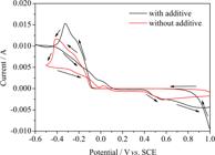
CV curves of ITO in electrolyte (a) with additive, (b) without additive, the scan rate: 0.01 V s-1.
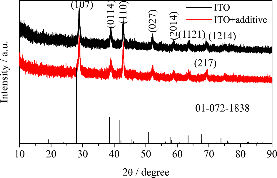
Figure 8 showed the XRD patterns of samples prepared in electrolytes containing and not containing additive on ITO substrate. As shown in Figure 8, the XRD patterns of the two samples were essentially identical, with all diffraction peaks corresponding to the reported (Bi0.5Sb0.5)4Te3, as listed in the standard card number (01 072-1838). It was showed that the additive did not alter the phase of the prepared Bi2-xSbxTe3 films. Compared to the standard card, all diffraction peaks shifted to the right, and the intensity of the (110) crystal plane diffraction peak increased, indicating preferential orientation at the (110) crystal plane. Generally, films prepared by electrodeposition tended to exhibited preferential orientation at the (110) crystal plane because the resistance was lowest at this position perpendicular to the substrate,30 which benefited conductivity and the deposition process.31 This differed from films prepared using physical or chemical techniques, which often exhibited preferential orientation at the (015) crystal plane.32,33
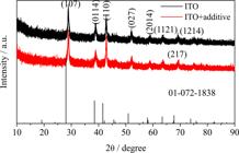
XRD patterns of the annealed Bi2-xSbxTe3 films in the electrolytes with or without additive.
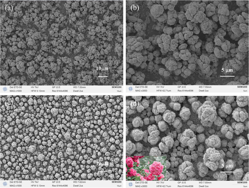
Figure 9 shows the SEM images of Bi2-xSbxTe3 films prepared on ITO substrates in electrolytes containing and not containing additive. As indicated in Figure 9, the morphologies of the two films were significantly different. Generally speaking, the deposition potential and the composition of electrolyte could severely affect the morphology of the constant potential deposited film.2,34 In this work, the deposition potential was kept constant. The only different condition was the addition of additive. Therefore, it could be concluded that the difference in surface morphology of the films was due to the addition of additive in the electrolyte.

The typical SEM images of the annealed Bi2-xSbxTe3 films prepared in the electrolyte without additive: (a) and (b), with additive: (c) and (d), and the insert was a typical rose flower picture.
As mentioned above, the Bi2-xSbxTe3 films prepared in an electrolyte without additive consisted of small particles and their agglomerations, as showed in Figure 9a. The microstructure of the Bi2-xSbxTe3 film exhibited a walnut-like shape, as illustrated in Figure 9b. After adding the additive, more nuclei formed in the electrolyte system, which was beneficial for forming a dense film. As shown in Figure 9c, the film became even denser. At the same time, it could also be observed that the Bi2-xSbxTe3 film was composed of irregular spherical small particles and larger particles formed by their agglomeration, with dimensions ranging approximately from 2 to 8 mm. From Figure 9d, it was evident that the microstructure of the Bi2-xSbxTe3 film presented a rose-like shape. It was clear that the addition of the additive increased the density of the prepared film and altered its morphology.
Performance of the as-prepared Bi2-xSbxTe3 films
In order to investigate the effect of substrate and additive on performance of the annealed ternary films, some parameters were measured. The thickness (h), electrical conductivity (σ), carrier concentration (n), and Hall mobility (μ) of the samples were given in Table 1.
From Table 1, a conclusion could be drawn that the sample 3 had the highest σ among three samples. This was ascribed to that the sample 3 had the most compact structure compared with samples 1 and 2. Meanwhile, the σ value of sample 3 was higher than the value of Bu et al.,30 but lower than that of Kim et al.22 because of different preparation methods or different preparation conditions. For example, the preparation in Kim et al.22 was potential-current co-adjusted pulse electrodeposition. Addition, the substrate was an Au-coated Si substrate. While in this work, the preparation was the potentiostatic electrodeposition and the substrate was ITO and SS. Furthermore, although the fabrication method in Bu et al.,30 was also potentiostatic electrodeposition and the substrate was SS, the SS was mechanically polished to mirror surface. Besides, the film deposited in Bu et al.,30 was three times thicker than that of as-fabricated in our work. This also decreased the value of σ than that of the films in our work. Surely, this made a difference. High σ value was good for obtaining high ZT value. Meanwhile, the sample 3 had the highest α among our three samples. The α value of our samples was lower than that of the films in Kim et al.22 but higher than that in Bu et al.,30 and Miyazaki et al.29 How to obtain the higher α value is our ongoing work.
Conclusions
In nitric acid solution, pure ternary (Bi0.5Sb0.5)4Te3 film could be successfully prepared by electrodeposition, whether ITO or SS was used as substrate. Substrate did not change the phase of the film. All the annealed films had granular structure, but the microstructure was quite different. The surface of the film prepared with ITO exhibited a “walnut kernel”-like morphology, while the surface of the ternary film prepared with SS presented a cauliflower-like morphology. Also, the addition of an additive did not change the phase of the (Bi0.5Sb0.5)4Te3 film. With the presence of the additive, the annealed film was denser, and the surface morphology exhibited a rose-like appearance. The results of the property test demonstrated that the annealed film prepared in the electrolyte with thiourea had the highest σ (984.50 S cm-1) compared with the films deposited in the electrolyte without thiourea or on the SS substrate. This work paves the way for theoretical support for crystal growth theory.
Acknowledgments
The authors gratefully acknowledge the financial support provided by the National Nature Science Fund of China under grant number (21873063), Shaanxi Provincial College Students Innovation and Entrepreneurship Plan Training Program (No. S202511396060), Qinchuangyuan “Scientist + Engineer” Construction Project in Shaanxi Province (2024QCY-KXJ-147).
Data Availability Statement
The data should be requested from the corresponding author.
References
-
1 Li, X. H.; Koukharenko, E.; Nandhakumar, I. S.; Tudor, J.; Beeby, S. P.; White, N. M.; Phys. Chem. Chem. Phys. 2009, 11, 3584. [Crossref]
» Crossref -
2 Li, S. H.; Toprak, M. S.; A Soliman, H. M.; Zhou, J.; Muhammed, M.; Platzek, D.; Müller, E.; Chem. Mater. 2006, 18, 3627. [Crossref]
» Crossref -
3 Li, G. R.; Zheng, F. L.; Tong, Y. X.; Cryst. Growth Des. 2008, 8, 1226. [Crossref]
» Crossref -
4 Yang, J. Y.; Zhu, W.; Gao, X. H.; Bao, S. Q.; Fan, X.; J. Electroanal. Chem 2005, 577, 117. [Crossref]
» Crossref -
5 Mao, J.; Chen, G.; Ren, Z. F.; Nat. Mater. 2020, 20, 454. [Crossref]
» Crossref -
6 Lu, Y.; Qiu, Y.; Cai, K. F.; Ding, Y. F.; Wang, M. D.; Jiang, C.; Yao, Q.; Huang, C. J.; Chen, L. D.; He, J. Q.; Energy Environ. Sci. 2020, 13, 1240. [Crossref]
» Crossref -
7 Lim, J. R.; Whitacre, J. F.; Fleurial, J. P.; Huang, C. G.; Ryan, M. A.; Myung, N. V.; Adv. Mater. 2005, 17, 1488. [Crossref]
» Crossref -
8 Purkayastha, A.; Kim, S.; Gandhi, D.; Ganesan, P. G.; Borca Tasciuc, T.; Ramanath, G.; Adv. Mater 2006, 18, 2958. [Crossref]
» Crossref -
9 Dresselhaus, M. S.; Chen, G.; Tang, M. Y.; Yang, R. G.; Lee, H.; Wang, D. Z.; Ren, Z. F.; Fleurial, J. P.; Gogna, P.; Adv. Mater 2007, 19, 1043. [Crossref]
» Crossref -
10 Wang, J.; Cai, K. F.; Yin, J. L.; Shen, S.; Synth. Met. 2017, 224, 27. [Crossref]
» Crossref -
11 Ni, D.; Song, H. J.; Chen, Y. X.; Cai, K. F.; Energy 2019, 170, 53. [Crossref]
» Crossref -
12 Yu, B. Y.; Duan, J. J.; Cong, H. J.; Xie, W. K.; Liu, R.; Zhuang, X. Y.; Wang, H.; Qi, B.; Xu, M.; Wang, Z. L.; Zhou, J.; Science 2020, 370, 342. [Crossref]
» Crossref -
13 Zhang, Y. H.; Peng, G. Y.; Li, S. K.; Wu, H. J.; Chen, K. D.; Wang, J. D.; Zhao, Z. H.; Lyu, T.; Yuan, Y.; Zhang, C. H.; Zhang, Y.; Ma, C. S.; Guo, S. W.; Ding, X. D.; Sun, J.; Liu, F. S.; Hu, L. P.; Nat. Commun. 2024, 15, 5978. [Crossref]
» Crossref -
14 Wu, X. Z.; Lin, Y. J.; Liu, C. Y.; Han, Z. J.; Li, H.; Wang, Y. P.; Jiang, F.; Zhu, K.; Ge, B. H.; Liu, W. S.; Adv. Energy Mater. 2023, 2301350. [Crossref]
» Crossref -
15 Moshwan, R.; Shi, X. L.; Liu, W. D.; Liu, J.; Chen, Z. G.; Nano Today 2024, 58, 102475. [Crossref]
» Crossref -
16 Wang, J. Y.; Gao, H. T.; Zhao, K. P.; Wuliji, H.; Zhao, B. R.; Ma, J.; Chen, X. Y.; Zhang, J. W.; Sui, Y. P.; Wei, T. R.; Zhu, M.; Shi, X.; Sci. Adv 2025, 11, eadt6298. [Crossref]
» Crossref -
17 Jiang, B. B.; Yu, Y.; Cui, J.; Liu, X. X.; Xie, L.; Liao, J. C.; Zhang, Q. H.; Huang, Y.; Ning, S. C.; Jia, B. H.; Zhu, B.; Bai, S. Q.; Chen, L. D.; Pennycook, S. J.; He, J. Q.; Science 2021, 371, 830. [Crossref]
» Crossref -
18 Han, C. G.; Qian, X.; Li, Q. K.; Deng, B.; Zhu, Y. B.; Han, Z. J.; Zhang, W. Q.; Wang, W. C.; Feng, S. P.; Chen, G.; Liu, W. S.; Science 2020, 368, 1091. [Crossref]
» Crossref -
19 Wu, C. L.; Shi, X. L.; Wang, L. J.; Lyu, W. Y.; Yuan, P.; Cheng, L. N.; Chen, Z. G.; Yao, X. D.; ACS Nano 2024, 18, 31660. [Crossref]
» Crossref -
20 Qiu, J. H.; Yan, Y. G.; Xie, H. Y.; Luo, T. T.; Xia, F. J.; Yao, L.; Zhang, M.; Zhu, T.; Tan, G. J.; Su, X. L.; Wu, J. S.; Uher, C.; Jiang, H. Y.; Tang, X. F.; Sci. China Mater. 2021, 64, 1507. [Crossref]
» Crossref -
21 Li, F. H.; Huang, Q. H.; Wang, W.; Electrochim. Acta 2009, 54, 3745. [Crossref]
» Crossref -
22 Kim, J.; Lee, K. H.; Kim, S. W.; Lim, J. H.; J. Alloys Compd. 2019, 787, 767. [Crossref]
» Crossref -
23 Qin, B. C.; Zhao, L. D.; Science 2022, 378, 832. [Crossref]
» Crossref -
24 Li, S. H.; A Soliman, H. M.; Zhou, J.; Toprak, M. S.; Muhammed, M.; Platzek, D.; Ziolkowski, P.; Müller, E.; Chem. Mater. 2008, 20, 4403. [Crossref]
» Crossref -
25 Liu, S. M.; Zhong, H. X.; Zhu, Y. H.; Guo, W. H.; He, Y.; Tian, C.; Wang, X. Q.; Shi, J. J.; Acta Mater. 2023, 255, 119045. [Crossref]
» Crossref -
26 Beyer, H.; Nurnus, J.; Bottner, H.; Lambrecht, A.; Wagner, E.; Bauer, G.; Physica E 2002, 13, 965. [Crossref]
» Crossref -
27 Aboulfarah, B.; Mzerd, A.; Giani, A.; Boulouz, A.; Pascal Delannoy, F.; Foucaran, A.; Boyer, A.; Mater. Chem. Phys. 2000, 62, 179. [Crossref]
» Crossref -
28 Hou, J.; Yang, J. Y.; Zhu, W.; Gao, X. H.; Functional Mater. 2006, 37, 1054. [Crossref]
» Crossref -
29 Miyazaki, Y.; Kajitani, T.; J. Cryst. Growth 2001, 229, 542. [Crossref]
» Crossref -
30 Bu, L. X.; Wang, W.; Wang, H.; Mater. Res. Bull 2008, 43, 1808. [Crossref]
» Crossref -
31 Wang, W. L.; Wan, C. C.; Wang, Y. Y.; Electrochem. Acta 2007, 52, 6502. [Crossref]
» Crossref -
32 Zou, H.; Rowe, D. M.; Min, G.; J. Cryst. Growth 2001, 222, 82. [Crossref]
» Crossref -
33 Damodara Das, V.; Selvaraj, S.; J. Appl. Phys 1999, 86, 1518. [Crossref]
» Crossref -
34 Yoo, B. Y.; Huang, C. K.; Lim, J. R.; Herman, J.; Ryan, M. A.; Fleurial, J. P.; Myung, N. V.; Electrochim. Acta 2005, 50, 4371. [Crossref]
» Crossref
Edited by
-
Editor handled this article:
Cristiane Luísa Jost (Associate)