Wideband Designs of E-shape Microstrip Antenna on Thinner Substrate
Abstract
Wider bandwidth microstrip antenna employing resonant slot require substrate thickness in excess of 0.07λg, which increases the antenna volume. In this paper, a novel technique to increase the bandwidth in E-shape microstrip antenna fabricated on a thinner microwave substrate, while employing printed resonator elements is proposed. The printed resonator positioned below the patch, introduces TM20 mode nearer to the TM10 mode in E-shape antenna that increases the bandwidth. On substrate thickness of 0.037λg, optimum design achieves bandwidth of 130 MHz (13.89%), with a broadside radiation pattern and peak gain of 7.8 dBi. With the obtained antenna characteristics, proposed thinner substrate designs will find applications in GSM band.
Index Terms
Broadband microstrip antenna; E-shape microstrip antenna; Thinner substrate design; Printed ring shape resonator.
I. INTRODUCTION
With numerous advantages like low profile planar design, microstrip antenna (MSA) finds wide applications in wireless systems [1], [2]. Initially MSAs were considered as narrow bandwidth (BW) elements. However, over the last four decades, many techniques have been developed to increase MSA BW. Of them, resonant slot cut method is the preferred one, as it maintains the low-profile single patch configuration [3], [4]. In slot cut designs, U-slot, pair of rectangular slots and their modified variations have been used, while using the coaxial or proximity or differential feeding [3] - [15]. The slot cut MSAs require substrate thickness ≥ 0.07λg, which increases the antenna volume, and the un-wanted radiation in the end-fire direction. Wideband design on thinner substrate discussed in [14] offers broadside radiation pattern but requires two U-slots and dual feeds. Modified ground plane designs on thinner substrates offer BW more than 70%, but they employ modifications in the patch and ground plane, thereby increasing the design complexity [16], [17]. Reduction in the antenna thickness is achieved by using the modified ground plane profile [18]. But they have lower gain, attributed to the increased back-lobe radiation. Although, coaxially fed slot cut technique to achieve BW improvement with a broadside gain is an optimum one, but it requires higher antenna thickness. Thus, there exists a research gap in designing coaxially fed wideband slot cut MSA on thinner substrate that offers a broadside radiation pattern, without significantly altering the gain characteristics.
In the present paper, a novel structure of coaxially fed E-shape MSA on thinner substrate, while employing proximity coupled printed resonator is proposed for a wideband response. The resonators are placed below the patch thereby not increasing the antenna dimensions. The proposed study initiates by highlighting the limitation of E-shape patch on reduced substrate thickness, to provide a wider BW. To realize broadband response on electrically thinner substrate, design of E-shape patch loaded with a printed open ring shape resonator is presented. A wider BW is realized through the mutual coupling between TM10 mode on E-shape MSA and TM20 mode on the ring shape resonator. Designs with single and two ring shape resonators are studied of which configuration employing two resonators offers maximum BW. On electrical substrate thickness of 0.037λg, it achieves reflection coefficient (S11) ≤ -10 dB BW of 130 MHz (13.89%), with a broadside radiation pattern and peak gain of 7.8 dBi. Design of E-shape MSA loaded with ring shape resonators on substrate thickness of 0.07λg is also presented that yields 7% BW increment. To highlight the novelty in the proposed design, a tabular comparison is presented ahead. The E-shape MSA is a widely reported design, but it requires a thicker substrate. The present study puts forward a technique that achieves wideband response in E-shape MSA with a reduction in thickness by 0.03λg. In terms of substrate thickness, gain and BW, proposed design offers optimum performance. With the obtained antenna characteristics, proposed designs can find applications in GSM band in 800 - 1000 MHz frequency range.
II. E-SHAPE MSA LOADED WITH RING SHAPE RESONATORS
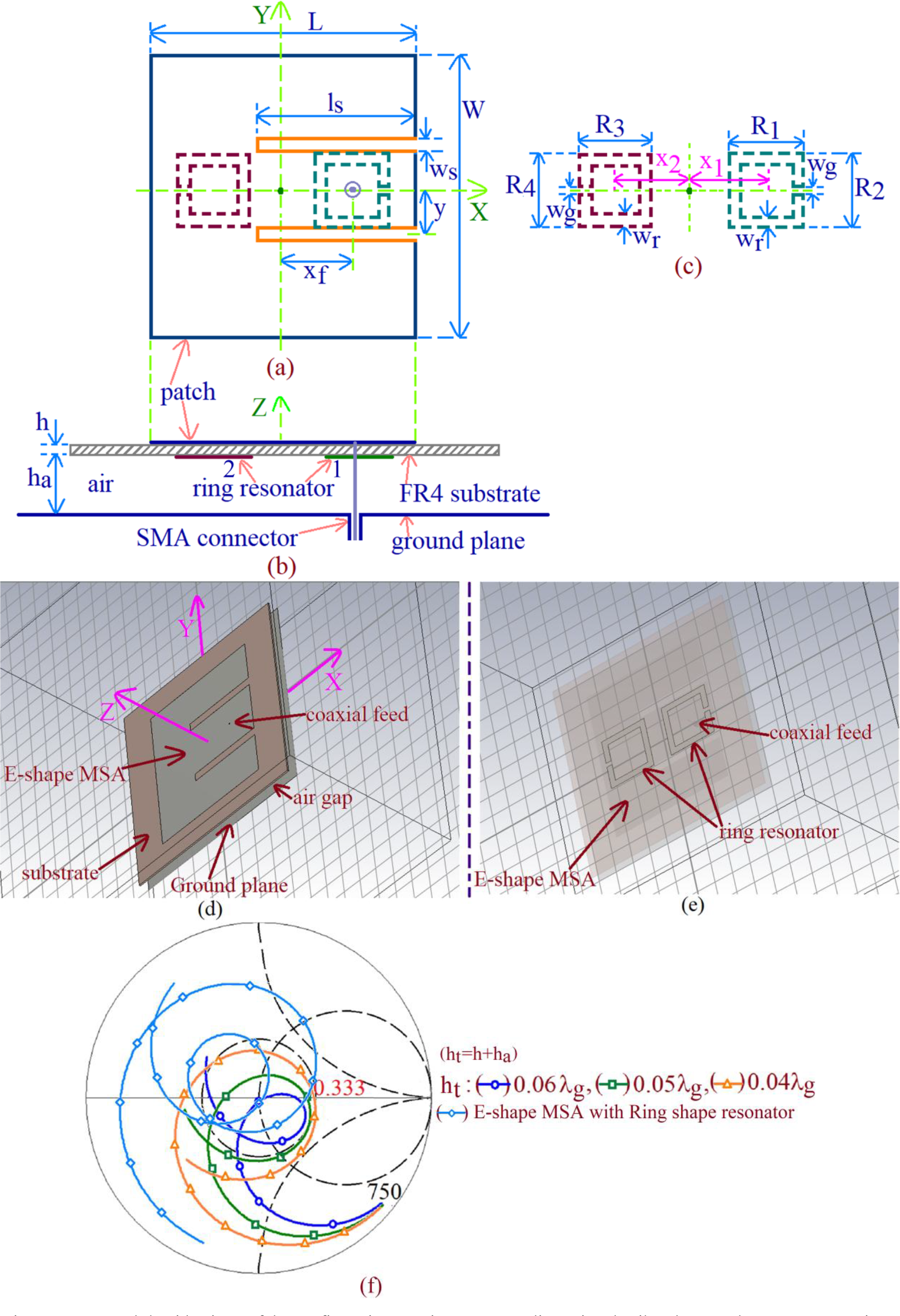
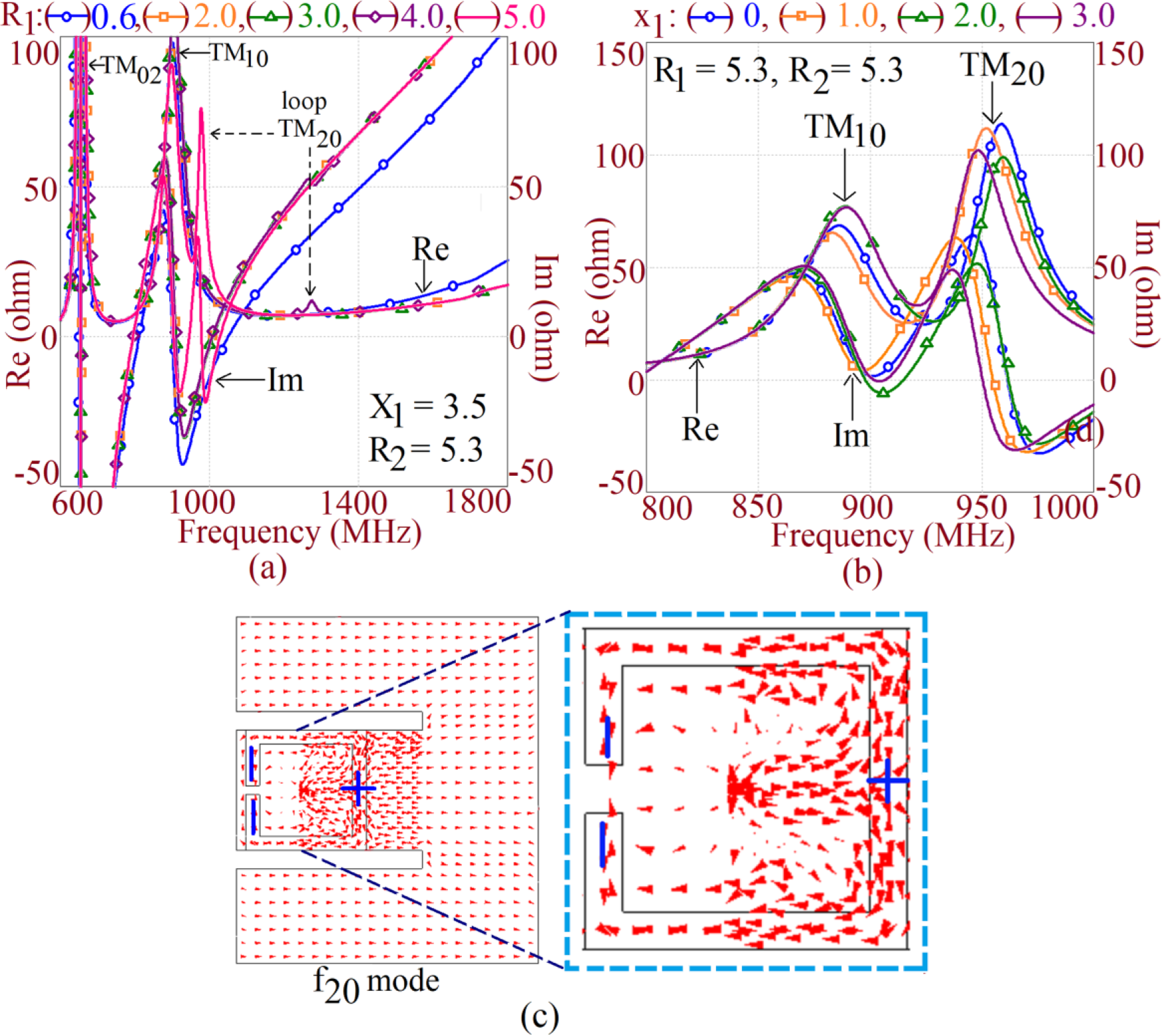
The coaxially fed wideband E-shape MSA is represented in Fig. 1(a, b). The patch is fabricated on FR4 substrate (εr = 4.3, h = 0.16 cm) that is suspended above the ground plane in air of thickness, ha = 2.0 cm. For the E-shape dimensions as, L = 13, W = 15, ls = 8.0, ws = 0.8, y = 3.0 cm, simulated BW is 196 MHz (22.14%). The substrate thickness with reference to the E-shape MSA’s TM10 mode frequency (892 MHz) is 0.067λg. The effect of reduction in total substrate thickness (ht) is studied and smith chart for the same are provided in Fig. 1(f). While reducing ht, ha is reduced. The impedance plots are shown for ha = 2.0, 1.5 and 1.2 cm, as mentioned in Fig. 1(f). With the reduction in ha, loop formed in the smith chart is not occupied completely inside VSWR = 2 circle, thus reducing the S11 BW. The BW can be increased, while ensuring more frequency points occupied inside VSWR = 2 circle. For this loop should be formed inside the circle, which requires addition of resonant mode in the antenna cavity. This is achieved by adding ring shape resonator, which is placed below the E-shape patch as mentioned in Fig. 1(a - e). For better representation, dimensional details of ring resonator are provided in Fig. 1(c). Also the 3D and component view obtained using CST model clearly showing the placement of ring resonators is provided in Fig. 1(d, e). For ha = 1.0 cm, initially only single ring shape resonator of dimension R1, R2 is placed below the pair of slots. The parametric study is carried out to investigate the effects of ring dimensions and its position x1 from the patch center. Resonance curve plots for the same are provided in Fig. 2(a, b). The plots are shown for R1 variation and for given R2. In E-shape MSA, wideband response is present around its TM10 mode [20].
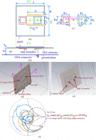
(a) Top and (b) side views of the configuration, (c) ring resonator dimension details, (d) 3D and (e) component views of CST model showing ring shape resonator placement in coaxially fed E-shape MSA loaded with ring shape resonators below the patch, and (f) smith chart for decreasing substrate thickness
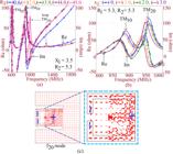
Resonance curve plots for variation in (a) R1 and (b) x1 for ring shape resonator, and (c) current distribution on ring resonator at TM20 mode for E-shape MSA loaded with ring shape resonators for ht = 1.16 cm
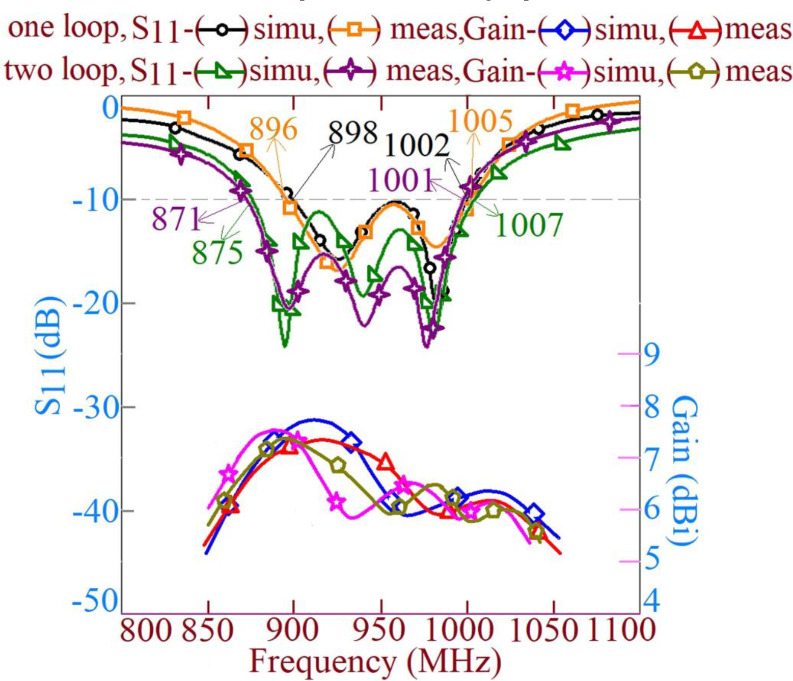
With an increase in R1, the frequency of the mode introduced by ring shape resonator reduces and gets tuned with respect to TM10 mode frequency. In the resonance plots provided in Fig. 2(a), R1 = wr (0.6 cm) means that only the vertical section of the ring resonator of dimension R2 and resonator strip width wr is present. In this parametric, the second resonator of dimensions R3, R4 is absent. An open circuit boundary condition is present towards the two ends on the ring resonator. With this, surface current shows two half wavelength variation on the ring shape, as given in Fig. 2(c). Hence, the resonant mode on printed ring shape resonator is referred to as TM20. Variation in ring position x1, displaces the position of ring resonator with reference to the patch center. In this variation, initially ring of dimension R1 = R2 = 5.3 cm is placed below and in the patch center and then value of x1 is increased. Position of ring alters the coupling between the patch and ring resonator mode that changes the impedance at them to provide optimum BW. Thus, parametric optimization in dimensions R1, R2, x1, yields loop position inside VSWR = 2 circle in the smith chart, as shown in Fig. 1(f) that enhances the BW on thinner substrate. Antenna parameters in the optimum design are, ha = 1.0, h = 0.16, R1 = R2 = 5.2, wg = 0.4, wr = 0.6, x1 = 3.5, xf = 3.6 cm and their results are shown in Fig. 3. For these antenna parameters, the left edge of ring shape resonator 1 is at a distance of 0.9 cm from the patch center.
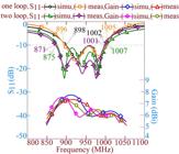
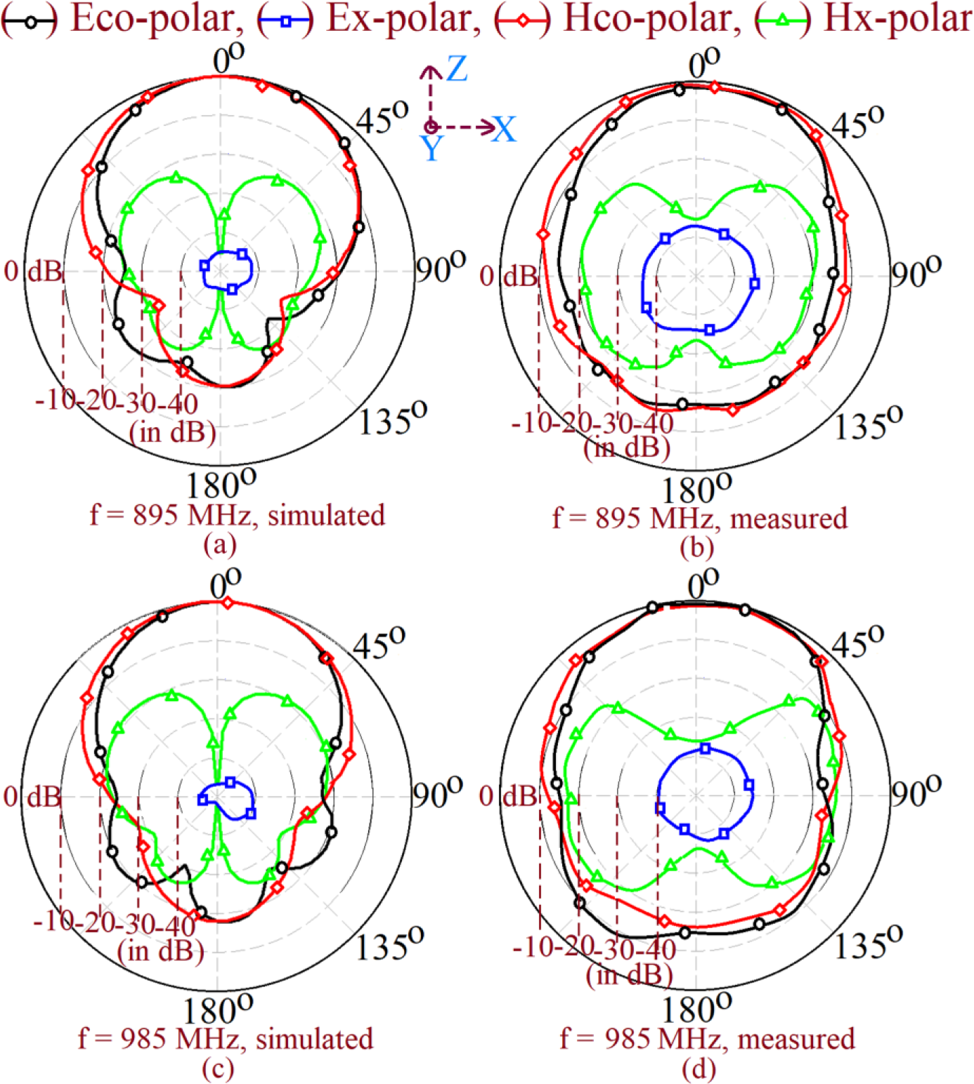
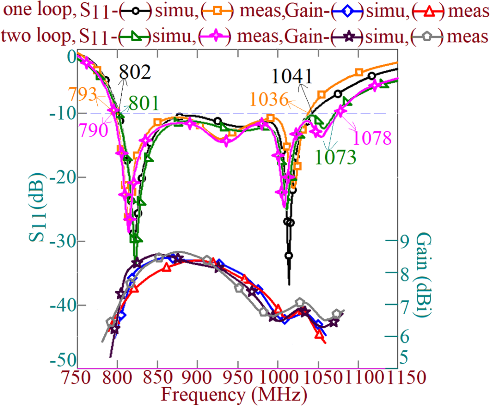
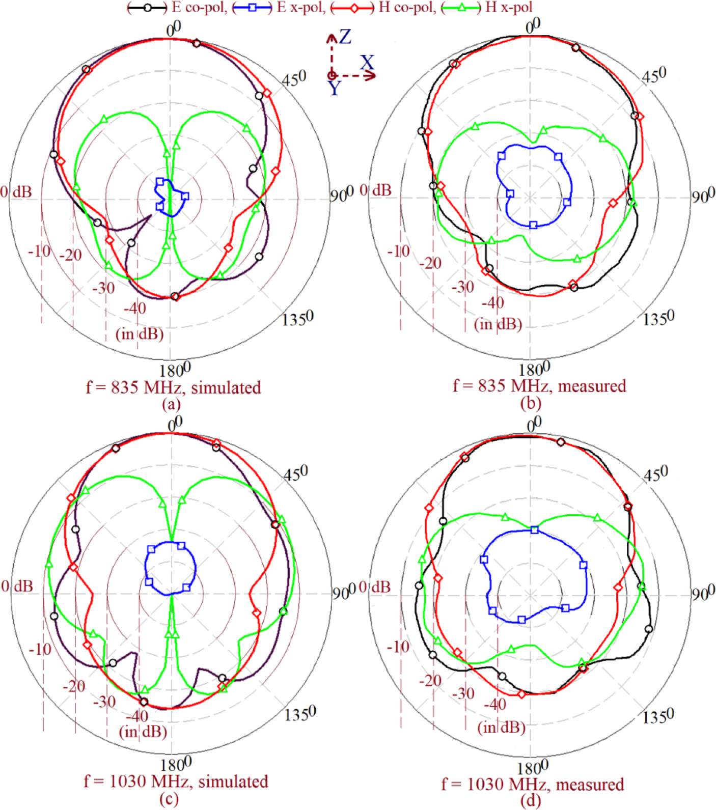
The antenna offers simulated and measured S11 BW of 104 MHz (10.95%) and 109 MHz (11.45%), respectively. The antenna gain is larger than 6 dBi over the complete BW with a maximum value of 7.8 dBi. The wideband MSA offers broadside radiation pattern. An increase in the BW is further achieved by loading second ring shape resonator below the E-shape patch, present on the other side of the first one. The second ring resonator is placed at a distance of x2 = 3.5 cm from the patch center. Only the parametric optimization in dimensions R3 and R4 is carried out to yield increase in the antenna BW. This is achieved for R3 = 5.2, R4 = 5.0, x2 = 3.5, xf = 3.6 cm and antenna yields simulated and measured S11 BW of 132 MHz (14.03%) and 130 MHz (13.89%), respectively as shown in Fig. 3. The right edge of the second ring resonator is present at distance of 0.9 cm from patch center, thus making the horizontal separation between the two resonators as 1.8 cm. The broadside antenna gain is larger than 6 dBi over most of the BW with a maximum value of 7.8 dBi. Radiation pattern plots nearer to the band edge frequencies of S11 BW are given in Fig. 4(a - d). The pattern at the frequencies shown and over the BW is in the broadside direction with cross-polar component of radiation less than 15 dB as compared with the co-polar radiation level. The E-plane is aligned along Φ = 00, across the BW.
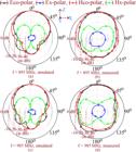
(a - d) Radiation pattern towards the band edge frequencies of the S11 BW for E-shape MSA loaded with two ring shape resonators for ht = 1.16 cm.
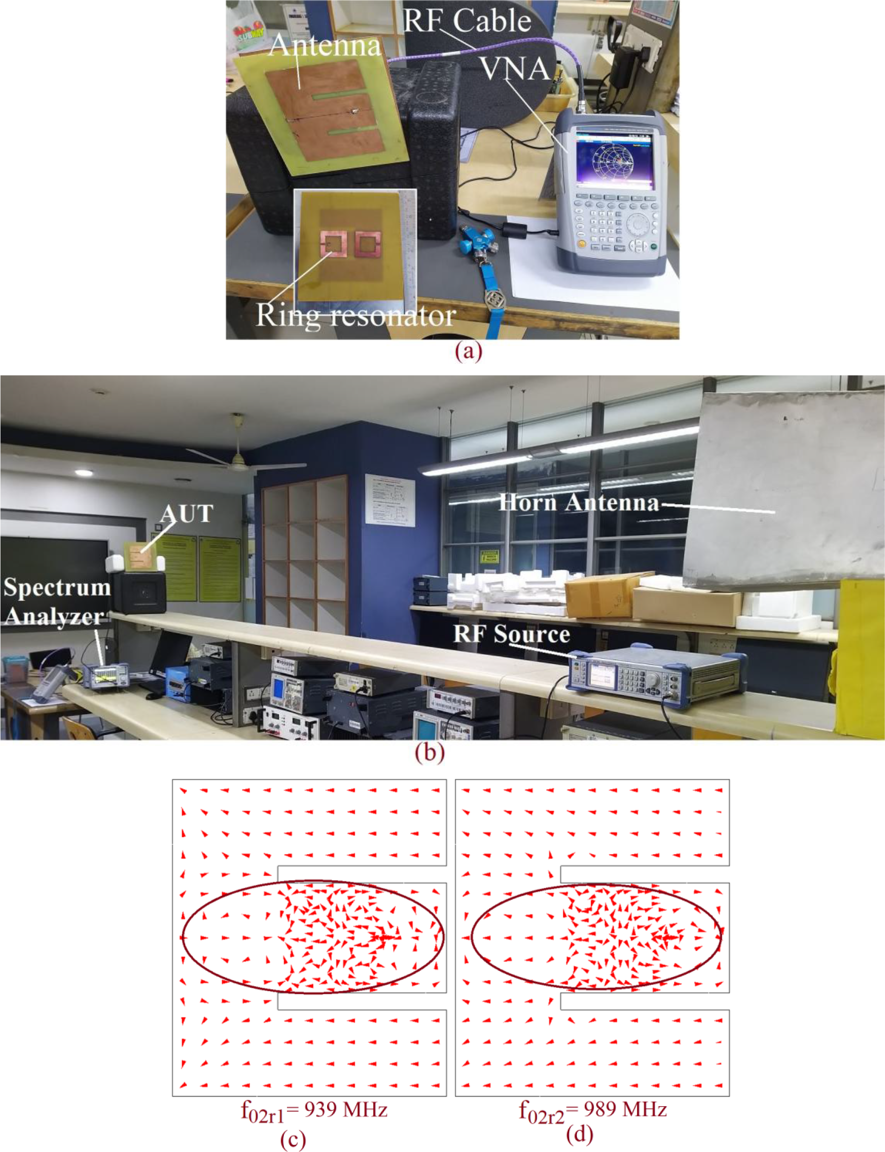
The configurations in this paper are initially optimized using CST software [19]. CST microwave studio is a high performance electromagnetic simulation software, which comprises of different solvers. In the present study time domain solver is selected. The 3D structure of the antenna drawn in CST is fed using waveguide port in combination with the coaxial feeding [19]. The fabricated antenna along with S11 BW measurement setup, radiation pattern and gain measurement setup is shown in Fig. 5(a, b). The antenna radiation pattern and gain are measured inside the antenna lab, wherein reference wideband and high gain Horn antenna were used. A required minimum far-field distance was maintained between the reference antenna and antenna under test (AUT). For a better accuracy in the lab measurement, three-antenna method is used in the broadside gain measurement.

(a) S11 BW and (b) gain measurement setup for E-shape MSA loaded with two ring shape resonators, (c, d) Surface current distribution at ring resonator modes
In single and two ring shape resonators loaded E-shape MSAs, variation in the broadside gain by 2 dBi from its peak value is noted across the S11 BW. This variation is observed at the frequencies where ring mode is present. As the ring resonator is placed below the patch, there exists a coupling between the two. When the resonant mode on ring is dominant, then surface currents on the patch gets affected and due to this vertical components of current vectors are observed on the E-shape MSA as shown in Fig. 5(c, d). Due to this gain varies towards those frequencies. However, across the BW it stays above 6 dBi, which is an appreciably large value from the practical applications. With respect to the center frequency of S11 BW, on substrate thickness of 0.037λg, proposed two ring shape resonator loaded design provides nearly 14% BW with a broadside radiation characteristics and peak gain of 7.8 dBi. These values are improved ones against the reported designs.
Employing the loading of ring shape resonators, BW in E-shape MSA is increased for total substrate thickness of 2.16 cm (0.067λg) as well, and results for them are provided in Fig. 6. For the above E-shape MSA dimensions, design parameters in a single ring shape resonator loaded configuration are, R1 = R2 = 5.2, x1 = 3.5, wg = 0.4, wr = 1.0 cm. It gives simulated and measured S11 BW of 239 MHz (25.94%) and 243 MHz (26.57%), respectively. With the loading of second ring shape resonator of dimension, R3 = 5.3, R4 = 5.2, x2 = 3.5 cm, E-shape MSA yields simulated and measured S11 BW of 272 MHz (29.03%) and 288 MHz (30.8%), respectively. The radiation pattern nearer to the band start and stop frequencies of the S11 BW in two ring shape resonators loaded E-shape MSA is shown in Fig. 7(a - d). In both the designs broadside radiation pattern across the S11 BW with a gain of more than 6 dBi is achieved. In comparison with a E-shape MSA for ha = 2.0 cm, two ring shape resonators loaded design offers BW increment by more than 7%, without any increase in the antenna volume.
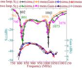
S11 BW and gain plots for E-shape MSA loaded with ring shape resonators on substrate thickness of 2.16 cm
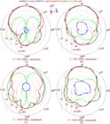
(a - d) Radiation pattern plots nearer to the band edge frequencies for E-shape MSA loaded with ring shape resonators on substrate thickness of 2.16 cm (0.067λg).
III. DESIGN METHODOLOGY FOR WIDE BAND E-SHAPE MSA
This section presents the design methodology for wideband E-shape MSA loaded with two ring shape resonators on thinner substrate. Initially resonant length formulation at TM10 and TM02 modes in rectangular MSA (RMSA) and TM20 modes in each ring shape resonator, which contribute to the S11 BW is presented. While doing the formulation, surface current distribution at the respective modes is extensively studied to arrive at each of the equation. The resonant length at TM10 mode in E-shape patch is given by using equation (1). The effective dielectric constant (εre) for ha = 1.0, h = 0.16 cm, εr = 4.3 is calculated by using equation (3) and the frequency is calculated using equation (2). The calculated frequency is 940 MHz that matches closely with the simulated value of 908 MHz.
At TM02 mode in equivalent RMSA, surface currents exhibit two half wavelength variation along the patch width. The effective patch width at the same is obtained by using equation (4) and the frequency is calculated using equation (5). For the antenna parameters present in the optimum design above, calculated frequency is found to be 1660 MHz that matches closely against simulated frequency of 1625 MHz.
The pair of slots in E-shape patch, reduces the resonance frequency of TM02 mode and its optimum spacing with respect to TM10 mode yields wider BW in E-shape design. The surface current paths at modified TM02 mode in E-shape MSA were studied and modified resonant length at TM02 mode is obtained by using equation (6). The frequency is calculated using equation (5) for W02 = We02. The calculated frequency is found to be 668 MHz against the simulated value of 657 MHz, thus providing a close match.
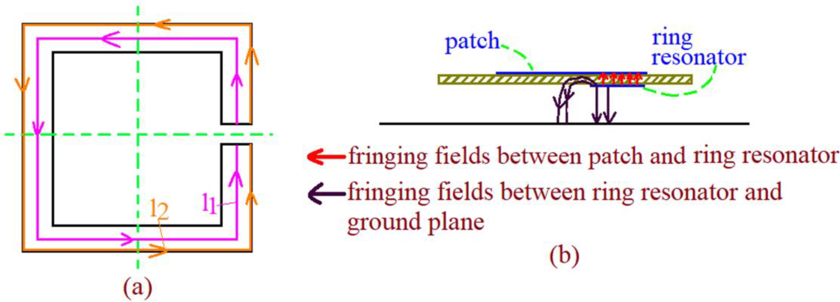
At TM20 mode in ring shape resonator, surface currents show two half wavelength variation along the total length. Amongst the two, ring shape resonator placed below the pair of slots is larger in dimensions and thus has lower resonance frequency. The resonant length at the ring shape resonator mode is obtained by taking the average of lengths l1 and l2 as mentioned in Fig. 8(a) and as given in equation (7). For the second resonator, R1 and R2 will get replaced by R3 and R4, respectively. The resonance frequency is calculated by using equation (8). The effective dielectric constant for ring shape resonator mode is obtained by using equation (9). For the ring resonator, E-shape patch with FR4 substrate is present on the top side, whereas air with ground plane is present on the bottom side. The fringing fields between the patch and ring resonator resides in the substrate and thus sees dielectric constant of the substrate (εr). Against this fringing fields between ring resonator and ground plane either passes through the substrate later through the air to the ground plane or passing through the air and terminating on the ground plane, as explained in Fig. 8(b).

(a) Average current paths and (b) fringing field distribution for the ring shape resonator mode
With this fringing field distribution, dielectric constant seen is that of the effective dielectric constant of substrate when suspended above the ground plane in air (εre). Thus, ring shape resonator see two values of dielectric constant on the two side, due to which average of these two values is considered as mentioned in (9). The TM20 mode frequency for the first ring shape resonator calculated using following equation is 951 MHz, which agrees closely with the simulated value of 940 MHz. For the second ring shape resonator, calculated frequency is 973 MHz that matches closely against simulated value of 987 MHz.
Using these formulations, procedure to design wideband E-shape MSA loaded with two ring shape resonators on thinner substrate is presented. In addition to the above formulations, various frequency relations those exists amongst various resonant mode frequencies in the optimum design above are used. The design methodology initiates by specifying the band start frequency (fst) of the desired S11 BW. Using the frequency relation as mentioned in (10), TM10 mode frequency of the patch is obtained. Further, using equation (11), total substrate thickness ht is evaluated. In this equation, value of εre is unknown, since air gap thickness is not available initially. An initial approximation for εre = 1.1 is considered. This value is based on the value of εre as present in the original design above. From this calculated value of ht, ha is selected, which is an integer number and practically realizable thickness. Using this value of air gap and for FR4 substrate, εre is re-calculated using equation (3). This new value is used in all further calculations. The patch length is calculated by using equation (12) and width is selected as W = 1.154L.
In the optimum design on thinner substrate, modified TM02 mode frequency bears a frequency relation, f02es = 0.751fst, with reference to the band start frequency of S11 BW. Using this modified patch width We02s is calculated by using equation (13). Further by using equation (14), slot length ls in the E-shape patch is evaluated. Equation (14) is obtained by re-arranging the terms on two sides of the equation (6). The slot position from the patch center is selected at y = 0.2W, whereas slot width is taken as, ws = 0.052W.
The TM20 mode frequency on the larger ring shape resonator bears a frequency relation, f20 = 1.071fst, with reference to the band start frequency of the S11 BW. Using this effective ring shape resonator length l20avg is calculated using equation (15). The effective dielectric constant as mentioned in (15) is calculated using equation (9). Further by using equation (16), ring shape resonator length R1 is obtained. Here, length R2 is taken equal to R1, whereas ring shape resonator strip width (wr) and gap between two arms (wg) are taken as 0.1154R1 and 0.0769R1, respectively. These dimensional relations have been used to simplify equation (7) that yields equation (16). The resonance frequency of TM20 mode on the second ring shape resonator is nearer to the TM20 mode frequency on the first resonator. Hence the vertical length of ring resonator is selected as, R4 = 0.9615R1. The horizontal length R3 equals R1, whereas dimensions of wr and wg are same as that present in the first ring resonator design. The two ring shape resonators are placed at a distance of x1 = x2 = 0.2692L from the patch center. The coaxial feed point is placed at a distance of xf = 0.2692L from the center of patch and inside the pair of slots, as mentioned in Fig. 1(a).
To validate the above design methodology, wideband MSA on thinner substrate loaded with two ring shape resonators is design for fst = 750 MHz, using FR4 substrate. Antenna dimensions calculated using the above procedure are, ha = 1.2, h = 0.16, L = 15.9, W = 18.3, ls = 9.6, y = 3.7, ws = 1.0, R1 = R2 = R3 = 6.2, R4 = 5.9, x1 = x2 = 4.3, xf = 4.3 cm. Antenna yields simulated and measured S11 BW of 92 MHz (11.75%) and 95 MHz (12%), respectively. Antenna offers broadside radiation pattern with a peak gain of greater than 7.5 dBi. Over the S11 BW, antenna gain remains above 6 dBi. The start frequency of the simulated BW is 737 MHz, which is close to the desired one. This validates the design methodology. Thus using the proposed methodology, similar thinner substrate wideband MSA can be designed around the given band start frequency that can be as per given practical application.
IV. COMPARATIVE ANALYSIS FOR THE PROPOSED OPTIMUM DESIGN
Wideband E-shape MSA on total substrate thickness of 1.16 cm yields optimum result as it requires thinner substrate amongst the proposed designs. Hence, to highlight on the novelty, results for the same are compared against the reported wideband designs mentioned in Table I. Patch area and substrate thickness mentioned in Table I are normalized with reference to the wavelength (λc) at the center frequency of S11 BW.
Initial reported wideband designs discussed in [3], [4] or multiple slots loaded designs presented in [10], [11] requires large substrate thickness. Thinner substrate design embedded with multiple slots on patch edges [5], dual slot design in [6] or differentially fed design presented in [7], has smaller BW. MSAs presented in [8], [9] does offer higher BW, but they employ differential feeding, modified patch shape, slot and shorting post, thus increasing the design complexity. Dual E-shape MSA presented in [12] has smaller BW for the equivalent value of the substrate thickness. Dual U-slot designs discussed in [13] and [14] either requires large antenna size or requires dual feed network. Designs considering modifications in the patch and ground plane do offer higher BW and gain [16], [17], but they are complex in design against the proposed configuration. MSA backed by a modified ground plane profile discussed in [18] offers lower peak gain, attributed to the increased back-lobe radiation. The proposed design employing ring shape resonators removes the necessity of modified ground plane profile to achieve wideband response on thinner substrate. Antenna size appears to be larger for the proposed design as compared with some of the reported configurations, since the proposed design is fabricated on air suspended lossy substrate against a thinner efficient but costly substrate used in the reported configurations. The use of air suspended substrate in the proposed design improves the reliability of antenna results against the substrate parameter variations. In the recent literature, array designs of E-shape MSAs [21], [22], modified E-shape patch using offset E-shape feed [23], [24], or E-shape patch loaded with U-slot for wideband high gain response [25], are reported. But in none of these papers, technique to reduce E-shape patch substrate thickness is being discussed.
To summarize, proposed study presents a simpler wideband E-shape design that offers BW enhancement for slot cut antenna on thinner substrate. As evident from the tabular comparison presented above, comparing the S11 BW, peak gain and antenna thickness together, proposed single coaxial feed design offers optimum performance against the reported wideband slot cut single patch configurations. Variation in broadside gain is observed, but it stays above 6 dBi, over the S11 BW. Thus, proposed study not just presents another wideband E-shape design, as reported more than two decades back, but a E-shape configuration that offers wideband response on thinner substrate, while employing a conventional ground plane. Design methodology proposed is helpful in designing similar wideband antenna as per given frequency band, which can be as per any given wireless application.
V. CONCLUSIONS
Wideband designs of E-shape MSA on thinner air suspended substrate, by employing printed ring shape resonators placed below the patch, and backed by conventional ground plane is proposed. The placement of resonators does not increase the patch size and maintains a low-profile configuration. Design employing two resonators offer optimum results, with S11 BW of 13.89%, broadside gain of more than 6 dBi, but on substrate thickness of 0.037λg. With the obtained antenna characteristics, proposed designs will find applications in GSM 800 - 1000 MHz frequency band.
REFERENCES
- [1] G. Kumar, K. P. Ray, Broadband Microstrip Antennas. Artech house, USA, 2003.
- [2] K. L. Wong, Compact and Broadband Microstrip Antennas. John Wiley and Sons, New York, USA, 2002.
-
[3] T. Huynh, K. F. Lee, “Single-layer single-patch wideband microstrip antenna”, Electronics Letters, vol. 31, no. 12, pp. 1310-1312, 1995, doi.org/10.1049/el:19950950.
» https://doi.org/doi.org/10.1049/el:19950950 -
[4] K. L. Wong, W. H. Hsu, “A broadband rectangular patch antenna with pair of wide slits”, IEEE Transaction on Antennas and Propagation, vol. 49, no. 9, pp. 1345-1347, 2001, doi:10.1109/8.951507.
» https://doi.org/10.1109/8.951507. -
[5] J. U. Yoo, H. W. Son, “A simple compact wideband microstrip antenna consisting of three staggered patches”, IEEE Antennas and Wireless Propagation Letters, vol. 19, no. 12, pp. 2038-2042, 2020, doi: 10.1109/LAWP.2020.3021491.
» https://doi.org/10.1109/LAWP.2020.3021491. -
[6] J. Wen, D. Xie, L. Zhu, “Bandwidth enhanced high-gain microstrip patch antenna under TM30 and TM50 dual-mode resonances”, IEEE Antennas and Wireless Propagation Letters, vol. 10, no. 10, pp. 1976-1980, 2019, doi: 10.1109/LAWP.2019.2935679.
» https://doi.org/10.1109/LAWP.2019.2935679. -
[7] C. Sun, “A design of low profile microstrip patch antenna with bandwidth enhancement”, IEEE Access, vol. 8, no. 10, pp. 181988-181997, 2020, doi: 10.1109/ACCESS.2020.3029219.
» https://doi.org/10.1109/ACCESS.2020.3029219. -
[8] X. Liu, H. Wei, G. Steven, W. Lehu, L. Qi, X. Rui, L. Ying, “A wideband triple-mode differentially-fed microstrip patch antenna”, IEEE Antennas and Wireless Propagation Letters, vol. 20, no. 7, pp. 1160-1164, 2021, doi: 10.1109/LAWP.2021.3074302.
» https://doi.org/10.1109/LAWP.2021.3074302. -
[9] S. Feng, Z. Li, W. Zibin, J. Yong-Chang, “A wideband differential-fed microstrip patch antenna based on quad-mode resonance with radiation patterns correction”, IEEE Transactions on Antennas and Propagation, vol. 71, no. 6, pp. 5404-5409, 2023, doi: 10.1109/TAP.2023.3255503.
» https://doi.org/10.1109/TAP.2023.3255503. -
[10] S. K. Sharma, L. Shafai, “Performance of a novel Ψ-shaped microstrip patch antenna with wide bandwidth”, IEEE Antennas and Wireless Propagation Letters, vol. 8, pp. 468-471, 2009, doi: 10.1109/LAWP.2009.2020184.
» https://doi.org/10.1109/LAWP.2009.2020184. -
[11] W. W. Li, Q. H. Li, Y. Meng, J. Y. Wang, W. M. Xu, “A broadband microstrip patch antenna with multiple open slots”, Microwave and Optical Technology Letters, vol. 61, no. 3, pp. 626-632, 2019, doi.org/10.1002/mop.31646.
» https://doi.org/doi.org/10.1002/mop.31646 -
[12] Q. Liu, L. Zhu, “A compact wideband filtering antenna on slots-loaded square patch radiator under triple resonant modes”, IEEE Transactions on Antennas and Propagation, vol. 70, no. 10, pp. 9882-9887, 2022, doi: 10.1109/TAP.2022.3184494.
» https://doi.org/10.1109/TAP.2022.3184494. -
[13] T. Q. Fan, B. Jiang, R. Liu, J. Xiu, Y. Lin, H. Xu, “A novel double U-slot microstrip patch antenna design for low-profile and broad bandwidth applications”, IEEE Transactions on Antennas and Propagation, vol. 70, no. 4, pp. 2543-2549, 2022, doi: 10.1109/TAP.2021.3125382.
» https://doi.org/10.1109/TAP.2021.3125382. -
[14] S. Radavaram, M. Pour, “Wideband radiation reconfigurable microstrip patch antenna loaded with two inverted U-slots”, IEEE Transactions on Antennas and Propagation, vol. 67, no. 3, pp. 1501-1508, 2018, doi: 10.1109/TAP.2018.2885433.
» https://doi.org/10.1109/TAP.2018.2885433. -
[15] Y. Chen, S. Yang, Z. Nie, “Bandwidth enhancement method for low profile E-shaped microstrip patch antennas”, IEEE Transactions on Antennas and Propagation, vol. 58, no. 7, pp. 2442-2447, 2010, doi: 10.1109/TAP.2010.2048850.
» https://doi.org/10.1109/TAP.2010.2048850. -
[16] S. Baudha, M. V. Yadav, “A novel design of a planar antenna with modified patch and defective ground plane for ultra-wideband applications”, Microwave and Optical Technology Letters, vol. 61, pp. 1320-1327, 2019, doi.org/10.1002/mop.31716.
» https://doi.org/doi.org/10.1002/mop.31716 -
[17] K. Mondal, P. P. Sarkar, “Gain and bandwidth enhancement of microstrip patch antenna for WiMAX and WLAN applications”, IETE Journal of Research, vol. 67, no. 5, pp. 726-734, 2021, doi.org/10.1080/03772063.2019.156595).
» https://doi.org/doi.org/10.1080/03772063.2019.156595 -
[18] A. A. Deshmukh, V. A. P. Chavali, A. G. Ambekar, “Thinner substrate designs of modified ground plane E-shape microstrip antennas for wideband response”, Electromagnetics, vol. 42, no. 4, pp. 255-265, 2022, doi.org/10.1080/02726343.2022.2099341.
» https://doi.org/doi.org/10.1080/02726343.2022.2099341 - [19] CST Studio Suite, “CST Microwave Studio”, Ver. 2019, 2019.
-
[20] A. A. Deshmukh, K. P. Ray, “Analysis of broadband Ψ-shape microstrip antennas”, IEEE Antennas and Propagation Magazine, vol. 55, no. 2, pp. 107-123, 2013, doi: 10.1109/MAP.2013.6529321.
» https://doi.org/10.1109/MAP.2013.6529321. -
[21] Y. Rahmatt-Samii, J. M. Kovitz, “Wideband E-shaped patch antennas for advanced wireless terminals”, Advanced Electromagnetics, vol. 12, no. 2, pp. 1-19, 2023, doi.org/10.7716/aem.v12i2.2191.
» https://doi.org/doi.org/10.7716/aem.v12i2.2191 -
[22] J. Taehwan, P. C. Soon, “60-GHz wideband L-probe circular slotted E-shaped patch antenna array”, IEEE Access, vol. 10, pp. 79939-79947, 2022, doi: 10.1109/ACCESS.2022.3194708.
» https://doi.org/10.1109/ACCESS.2022.3194708. -
[23] T. Latha, R. Gopi, A. K. Gande, M. Chakravarthy, “Compact wideband E-slotted E-shaped patch antenna for Ku-band phased array applications”, IEEE Transactions on Aerospace and Electronic Systems, vol. 60, no. 4, pp. 5596-5603, 2024, doi: 10.1109/TAES.2024.3374275.
» https://doi.org/10.1109/TAES.2024.3374275. -
[24] B. A. Sheik, P. V. Sridevi, P. V. Rama Raju, “E-shape patch antennas for multitasks/uninterrupted 5G communuication”, Wireless Personal Communication, vol. 10, pp. 873-891, 2020, doi.org/10.1007/s11277-019-06761-9.
» https://doi.org/doi.org/10.1007/s11277-019-06761-9 -
[25] D. K. Naik, A. K. Sahu, R. K. Parida, P. Raiguru, D. C. Panda, R. K. Mishra, “Design of a broadband U-slot loaded E-shaped patch antenna using characteristics mode analysis”, AEU - International Journal of Electronics and Communication, vol. 154, pp. 1-8, 2022, doi.org/10.1016/j.aeue.2022.154310.
» https://doi.org/doi.org/10.1016/j.aeue.2022.154310