 AsSe-free Si–Te–Ge chalcogenide glass OTS selectors designed by interpretable machine learning
ABSTRACT
Developing environmentally benign volatile switches for high-density memory arrays requires eliminating toxic arsenic and selenium without compromising thermal or electrical reliability. This study implements an interpretable machine learning framework to guide the compositional optimization of ternary chalcogenide systems. By leveraging SHAP feature analysis, we identified that a specific atomic balance is required to optimize network connectivity while maintaining high polarizability. Experimental validation of the ML-designed candidates revealed that a symmetric modifier ratio of Si10Ge10Te80 yields the most robust amorphous network, achieving a crystallization temperature of 235 °C and an optical bandgap of 1.05 eV. Electrical characterization of crossbar devices utilizing this composition demonstrates excellent volatile switching behaviors, characterized by a sharp threshold voltage of 1.25 V and an extremely low off-state leakage current of 5.3 × 10⁻⁸ A. Furthermore, the optimized device exhibits superior dynamic performance, featuring a fast switching speed of approximately 12 ns and high endurance exceeding 108 cycles, significantly outperforming silicon-rich variants which failed near 105 cycles due to devitrification. The findings confirm that controlling the average valence electron concentration around 5.1 allows for the suppression of leakage pathways while ensuring sufficient thermal stability, proving that data-driven material selection can effectively engineer high-performance, eco-friendly components for next-generation storage class memory.
Keywords:
3D crosspoint memory; Thermal stability; Leakage current; Switching endurance; SHAP analysis
1. INTRODUCTION
Modern high-density memory technologies such as 3D crosspoint phase-change memory (PCM) demand reliable two-terminal selector devices to suppress sneak-path leakage currents in large resistor networks [1]. Ovonic threshold switching as a physical phenomenon has a much longer history than recent selector-application papers might suggest. The reversible ‘threshold’ transition in amorphous chalcogenides was discovered by S. R. Ovshinsky in the early 1960s, well before modern storage-class memory concepts, and it became a foundational example of rapid electronic switching in disordered semiconductors. In this classic behavior, the amorphous film remains highly resistive until the applied field reaches a critical threshold, after which the conductivity increases abruptly and then returns to the high-resistance state when the current is reduced below the holding condition, enabling true volatile switching rather than nonvolatile phase transformation [2]. Over the past decade-plus, this phenomenon has been actively engineered into two-terminal selector devices for dense crosspoint arrays, where suppressing sneak-path currents is essential for scalability. Multiple research groups have systematically developed selector-optimized chalcogenide compositions, device stacks, and reliability strategies, and the field has matured into a well-established selector technology landscape rather than an emerging topic. Reviews and mechanistic studies have summarized key milestones, including the materials families, selector requirements, and the main classes of proposed switching mechanisms [3]. In parallel, Te-based selector materials have been widely studied because Te-rich networks can enable low threshold voltages and high current drive, although thermal stability is often a limiting factor; notable work from imec and collaborators mapped Te-based selector composition–property space and demonstrated practical routes to raise crystallization temperature through compositional tuning and Si incorporation [4]. In an OTS device, the amorphous chalcogenide remains highly resistive (off-state) until a threshold voltage (Vth) is applied; beyond this point, the material enters a conductive on-state until the voltage falls below a hold value (Vhold), returning the device to off-state [5]. An initial higher “first-fire” voltage (Vff) is often needed to condition the device.
Historically, the highest-performing OTS materials have included elements like arsenic (As) and selenium (Se) as glass formers (e.g. As–Se–Ge or As–Te–Ge systems) [6]. While such As/Se-based chalcogenide glasses can exhibit excellent threshold switching characteristics, their use raises concerns due to the toxicity and regulatory restrictions on As and Se in semiconductor manufacturing [7]. However, As still introduces additional environmental, health, and safety burdens during thin-film processing and waste handling, and occupational guidance highlights exposure concerns in GaAs-related microelectronics processing. In the OTS selector literature specifically, As is widely recognized as historically improving glass stability and switching performance, but its toxicity is also a primary motivation for developing As-free selector stacks suitable for high-volume integration [8]. Therefore, our goal in this work is not to claim that As-containing materials cannot be used, but to demonstrate that comparable selector performance can be achieved in an As/Se-free material system that may reduce EHS complexity while maintaining reliability. Therefore, there is strong motivation to develop AsSe-free OTS selectors that eliminate these hazardous elements without compromising device performance [9]. Recent studies have explored various As/Se-free chalcogenide systems as alternative OTS materials, notably Te-based binary and ternary alloys such as B–Te, C–Te, Si–Te, Ge–Te, Zn–Te, Ag–Si–Te, Mg–Te, Ge–C–Te, Hf–O–Te, as well as S-based glasses like Ge–S [10]. Many of these As/Se-free candidates have demonstrated the requisite nonlinear I–V behavior, but they often face challenges in terms of thermal stability or endurance under repetitive switching [11]. For example, pure Te-based selectors can achieve high on-current densities (>10 MA/cm2) and decent cycling endurance [12], but Te films tend to crystallize at relatively low temperatures (~150 °C), causing elevated leakage current (Ioff) and limiting reliability. Meanwhile, S-rich glasses like Ge–S can offer ultra-low Ioff and high thermal stability above 350 °C, yet their threshold voltages are relatively high (≥3 V) [13]. Striking a balance between low leakage, low switching voltage, and high thermal endurance remains a central materials challenge in OTS research [14]. From an integration viewpoint, selectors are fabricated as thin films within dense crossbar stacks, so reducing hazardous constituents can simplify fab handling protocols and end-of-life considerations while still meeting electrical and thermal requirements.
Among As/Se-free compositions, the ternary Si–Te–Ge system has emerged as a promising matrix for OTS selectors. Germanium and tellurium form the backbone of many phase-change materials and selectors: Ge–Te alloys (particularly Te-rich ones) are known to exhibit threshold switching (e.g. amorphous GeTe6 shows threshold switching at nanosecond scales) but tend to have crystallization temperatures below ~250 °C, which is problematic for the ≥400 °C backend-of-line (BEOL) thermal budget [15]. Incorporating lighter, tetrahedral network-formers like silicon into Te-based glasses can strengthen the amorphous network and raise thermal stability. In fact, ab initio simulations and experiments indicate that replacing or partially substituting Ge with Si in Te-rich glasses increases the glass transition and crystallization temperatures significantly [16]. Amorphous Si–Te (a-SiTe) binary glass has been shown to possess a highly resilient random network structure: over 76% of Si atoms in a-SiTe adopt fourfold tetrahedral coordination (obeying the 8−N rule) versus more defective structures in a-GeTe, which leads to a much higher resistance against crystallization in Si–Te glasses [17]. This inherent structural stability of Si–Te glass is beneficial for OTS selectors, preventing undesired devitrification under prolonged electrical stress or heat. However, pure Si–Te devices typically exhibit higher threshold voltages and slightly lower on-state currents compared to Ge–Te devices [18], owing to the increased average bond strength and wider bandgap introduced by Si. A recent study by WU et al. [12] found that increasing Si content in binary Si–Te selectors markedly reduces the off-state leakage (by over an order of magnitude) but concomitantly raises Vth by about 0.5–1 V. Conversely, Ge-rich glasses yield lower Vth but higher Ioff and lower thermal stability [19]. These observations suggest that an optimal composition in the Si–Te–Ge ternary phase space could harness the advantages of both Si and Ge: combining Si’s network-stabilization (low Ioff, high Tx) with Ge’s ease of electronic excitation (low Vth).
To rationally design such an optimal AsSe-free Si–Te–Ge OTS material, we employ an interpretable machine learning (ML) approach alongside experimental exploration [20, 21]. Data-driven modeling is increasingly used to accelerate glass development by uncovering composition–property relationships that may elude intuition [22]. This approach is motivated by a practical bottleneck widely recognized in selector development: the compositional search space grows combinatorially with each added element, while device qualification requires many coupled measurements (thermal stability, leakage under bias, switching speed, and endurance) [3]. As a result, the cost of purely empirical screening can become prohibitive even for ternary systems. Data-driven composition–property modeling has therefore become a common strategy to reduce experimental burden and to prioritize candidates with a higher probability of meeting multiple constraints simultaneously. In glass and inorganic materials more broadly, large-scale datasets have been used to train composition–property models, and interpretable techniques (including SHAP and related game-theoretic explanations) have been adopted to extract human-readable rules instead of opaque predictions [23]. In particular, we leverage a dataset of known chalcogenide compositions and their properties to train ML models predicting key OTS metrics (e.g. Vth, Ioff, thermal stability). Rather than a “black box”, we use interpretable ML tools (such as SHAP value analysis) to identify which features (e.g. atomic fractions, average coordination number, electronegativity, etc.) most strongly influence the selector performance [23]. This guided our selection of several candidate Si–Te–Ge compositions for synthesis and testing. In this work, we report the fabrication and comprehensive characterization of AsSe-free Si–Te–Ge OTS selectors designed via interpretable ML. We present a systematic comparison of material structure, optical/electrical properties, and device performance for a series of Si–Te–Ge glass films with varying Si:Ge ratio (all with high Te content to ensure threshold switching behavior). Using a combination of spectroscopic and microscopic techniques (FTIR, XRD, SEM, TEM, XPS, UV–Vis, BET surface area, etc.), we elucidate how Si and Ge substitutions affect the amorphous structure and electrical switching properties. We also evaluate device performance (I–V characteristics, threshold voltage, off-current, endurance, and scalability) for each composition. Finally, we apply our ML model to interpret the experimental trends, providing human-interpretable design rules for optimizing OTS materials. The insights from this study demonstrate a viable As/Se-free selector glass that meets the stringent requirements of memory selectors, and more broadly, highlight the power of combining machine learning guidance with materials science in developing next-generation electronic materials.
2. MATERIALS AND METHODS
Glass Fabrication: High-purity Si–Te–Ge chalcogenide glasses were prepared by a two-step process of melt-quenching (for bulk synthesis) followed by thin-film deposition (for device integration). In the bulk step, mixtures of 5N purity elemental Ge, Si, and Te in the desired atomic ratios were sealed in evacuated quartz ampoules (10−5 Torr). The mixtures were heated to 950 °C and homogenized for 12 h, then water-quenched to yield solid bulk glasses. Five target compositions were synthesized, labeled STG-0 through STG-4. These compositions span from a Ge-rich endmember (STG-0) to a Si-rich endmember (STG-4), all with Te as the majority component. For example, STG-2 is a balanced Si–Ge composition (≈10 at.% each of Si and Ge, rest Te). We first synthesized melt-quenched Si–Te–Ge bulk glasses. These bulk ingots served as composition-verified references and as DSC specimens; they were not a prerequisite for forming the device films. Mixtures of 5N purity Ge, Si, and Te were sealed in evacuated quartz ampoules (10−5 Torr), heated to 950 °C for 12 h to homogenize, and water-quenched to obtain bulk glasses. The bulk compositions were confirmed by EDS on polished samples.
Film Deposition: Thin films (~100 nm thick) of each glass were deposited on substrates for characterization and device fabrication. A radio-frequency magnetron co-sputtering technique was employed, using high-purity Si, Ge and Te targets in an argon plasma. By adjusting the relative RF power on the Si and Ge targets, the composition of the co-sputtered film was tuned to match each bulk glass composition [24]. OTS device films were deposited by RF magnetron co-sputtering from elemental Si, Ge, and Te targets. Because multi-target sputtering can require calibration due to different sputter yields, we used the bulk-glass compositions as targets for power calibration and then adjusted the RF powers to reach the desired Si:Ge ratio. Film compositions were verified directly on the deposited layers by EDS, and only composition-confirmed films were used for subsequent structural, thermal, and electrical analyses. A fully thin-film-only workflow is also feasible provided equivalent composition calibration/verification and thermal-stability characterization are implemented. All films were deposited at room temperature on 300 nm SiO2/Si substrates for material characterization, and on patterned TiN electrode wafers for device fabrication. The deposition system base pressure was <5 × 10⁻⁷ Torr, and a low sputtering power density was used to ensure amorphous, uniform films. Film thickness and uniformity were monitored by a quartz crystal microbalance and verified by cross-sectional scanning electron microscopy (SEM). EDS was performed on each film, confirming that the film compositions matched the intended Si–Te–Ge ratios (within experimental error), with negligible contamination (O and C < 0.2 at.%).
Device Fabrication and Testing: For electrical characterization, prototype OTS devices were fabricated in a crossbar configuration. Using the co-sputtered films, ~10 nm thick Si–Te–Ge layers were deposited on lithographically defined bottom electrodes (TiN) of various diameters (60–200 nm) on SiO2/Si substrates [25]. After chalcogenide deposition, a 40 nm TiN top electrode was sputtered, completing the MIM device stack [26]. The top electrode was patterned into pads using a lift-off process aligned to the bottom electrode via electron-beam lithography for the smallest devices. The resulting devices had the structure: TiN bottom electrode/10 nm Si–Te–Ge/TiN top electrode. We fabricated devices for each glass composition on the same wafer to enable direct performance comparisons.
Electrical testing was conducted using a Keithley 4200A-SCS parameter analyzer for DC sweeps and a Tektronix MSO54 oscilloscope for pulsed measurements. All measurements were done at room temperature. For DC I–V characterization, the two-terminal devices were biased in series with a 1 kΩ load resistor to limit current (protecting against damage during threshold switching). We employed both unipolar sweeps and alternating polarity sweeps to evaluate threshold switching and check for any non-volatility. The threshold voltage (Vth) was defined as the turn-on voltage at the onset of snapback (i.e., the peak voltage immediately before the abrupt transition from the high-resistance branch to the low-resistance branch in the voltage sweep). Because the apparent snapback trajectory can be influenced by the external load line and compliance settings, we additionally report an operational metric V(1 μA), defined as the applied voltage at which the current first reaches 1 μA during the off-to-on transition, to enable robust comparison across devices measured under the same setup. The holding voltage (Vhold) was extracted during the reverse sweep when the device returns to the high-resistance state. The off-state leakage current Ioff was measured at ½ Vth bias. A compliance current of 100 μA or 30 μA (for sub-100 nm devices) was set to prevent excessive heating. For pulsed tests, triangular voltage pulses of 1 μs rise/fall were applied to evaluate dynamic switching. Endurance testing was performed by applying successive threshold-switching pulses until device failure criteria were met.
Machine Learning Analysis: We assembled a dataset of ~60 known chalcogenide compositions labeled with properties relevant to OTS performance: threshold voltage, off-current, thermal stability (Tx or Tg), etc. Using this dataset, we trained gradient-boosted decision tree models (XGBoost) to predict Vth and log(Ioff) from features such as composition (at.% of Si, Ge, Te, and any other elements in literature entries), average number of valence electrons (Nve), average atomic radius, electronegativity differences, and bandgap. Model hyperparameters were optimized via 5-fold cross-validation. Although our dataset was modest, the models achieved decent predictive accuracy (R2 ~0.8 for Vth), sufficient for qualitative insights. To interpret the models, we employed SHAP (SHapley Additive exPlanations) analysis [27]. SHAP values were computed for each feature to quantify its influence on the predicted output. This allowed us to rank features by importance and visualize how changes in a feature (e.g. increasing Si content or Te content) impact Vth or Ioff in the model’s learned relationships. We paid special attention to features like Nve, since prior studies indicated that effective OTS glasses satisfy an “average 5 valence electrons rule” (Nve ≈ 5.0 ± 0.3 corresponds to optimal trap formation and threshold switching). The ML model results were used as a guiding framework to explain our experimental observations in the Results and Discussion.
3. RESULTS AND DISCUSSION
3.1. Composition and structure
The five Si–Te–Ge glass compositions studied are summarized in Table 1. As-designed atomic fractions are listed, along with the characteristic temperatures Tg and Tx determined by DSC. All compositions have a total of 10–20 at.% group IV elements (Si+Ge) with the balance Te, and all satisfy the 5 ± 0.3 average valence electron criterion for OTS materials [28]. We note that Nve for these glasses ranges between 5.0 and 5.3, which falls in the typical range of known OTS selectors like Si–Ge–As–Te. Experimentally, all films were amorphous as deposited. XRD patterns exhibit only broad humps around 2θ ~ 25–30°, with no crystalline peaks for any Si–Te–Ge sample, confirming the fully amorphous structure. In contrast, a control film of pure Te showed sharp diffraction peaks of trigonal Te [29], indicating that elemental Te would crystallize during deposition, whereas the addition of Si and/or Ge successfully yields an amorphous solid solution. This is a crucial result: incorporating even a small fraction (~5–10 at.%) of Si or Ge is sufficient to glassify Te, avoiding crystallinity.
From Table 1, we see a non-monotonic trend in thermal stability across the series. The crystallization temperature Tx peaks at ~235 °C for the STG-2 composition (Si ≈ 10, Ge ≈ 10) and decreases toward the end-member compositions. With the corrected DSC reporting, the lowest Tx in this series is observed for STG-0 (~165 °C), while STG-4 shows Tx ~170 °C. This preserves the main conclusion that an intermediate Si:Ge balance maximizes thermal stability. Consistent with common practice in chalcogenide-glass analysis, the thermal-stability window can be discussed using ΔT = Tx − Tg, which is positive for all compositions and reflects resistance to devitrification during heating. This trend mirrors what was observed in the binary Si–Te system by WU et al. [12]: the crystallization temperature was only 78 °C for a 1:1 SiTe binary, rose to ~235 °C at an intermediate Si:Te ~1:2 composition, then dropped again as Si was further reduced. In our ternary, the presence of Ge shifts the glass stability optimum toward a more balanced Si:Ge ratio. STG-2 (10% Si, 10% Ge) shows the highest thermal stability, with Tx = 235 °C and also the highest Tg = 183 °C. This is a promising sign, as 235 °C exceeds the typical phase-change memory operating ambient and approaches BEOL limits. The drop in Tx for STG-3 and STG-4 suggests that too little Ge can be detrimental, possibly because the glass becomes Te-poor in tetrahedral formers (Si or Ge) and may phase-separate or crystallize more easily. At the Si-rich end, the material likely crystallizes into Si2Te3 or similar phases at lower temperature (SiTe’s Tx was only 78 °C in binary). On the Ge-rich end, although Ge helps reduce Vth, it also introduces structural units (GeTe4 tetrahedra or defective octahedra) that are less effective at raising Tx than Si is [30]. Thus, the intermediate Si–Ge balanced composition achieves the best network connectivity and rigidity, maximizing thermal stability.
Structurally, FTIR and Raman spectroscopy provided further insight. The FTIR spectra of all samples were largely featureless in the 400–1000 cm−1 region, without sharp vibrational bands (Figure 1(a)). This is expected for amorphous network solids lacking distinct molecular vibrations. A very weak broad absorption around ~1200 cm−1 was noted for Ge-containing samples, which could be attributed to Ge–Te stretching modes or trace Ge–O bonds. However, the absence of a strong ~800–900 cm−1 band indicates negligible Ge–O content [31]. Raman spectra similarly showed broad bands rather than sharp peaks (Figure 1(b)). A diffuse band around 150 cm−1 (especially in Ge-rich STG-0) can be assigned to Te–Te chain vibrations, while a band near 250 cm−1 emerges with higher Si content, likely from symmetric stretching of Si(Te)4 units or mixed Si/Ge–Te vibrations. These trends qualitatively match known Raman signatures in Ge–Te and Si–Te glasses. In summary, the vibrational spectroscopy confirms an amorphous network with predominantly heteropolar bonds (Si–Te, Ge–Te) and a lack of any oxide or molecular impurity phases.
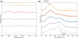
(a) FTIR spectra of the five Si–Te–Ge amorphous thin films (STG-0 to STG-4). (b) Raman spectra showing broad, non-crystalline vibrational bands characteristic of fully amorphous chalcogenide networks.
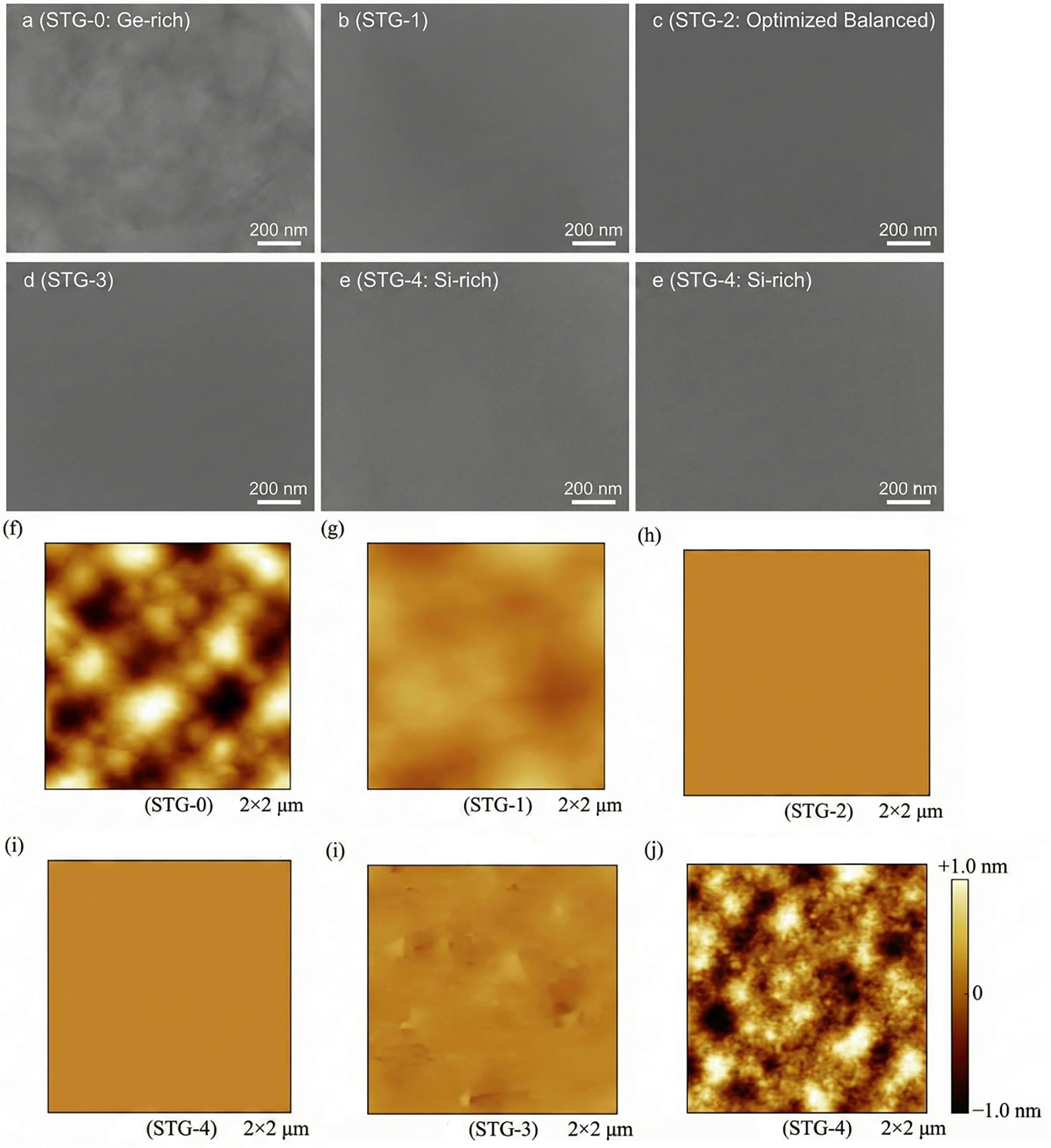
Top-view FESEM images of all Si–Te–Ge films reveal smooth, featureless surfaces without discernible grain boundaries, voids, or phase-segregated domains (Figure 2(a)−(e)). Even at high magnification (≥100,000×), the films exhibit a dense and continuous morphology, indicating uniform film growth during sputtering. No evidence of columnar growth or island formation is observed, suggesting that the low-power RF sputtering conditions effectively suppressed surface diffusion–driven crystallization. In contrast to pure Te films, which typically show faceted grains and needle-like features due to spontaneous crystallization [32], all Si–Te–Ge compositions remain morphologically amorphous, consistent with the XRD results. Notably, the Ge-rich STG-0 sample exhibits slightly higher surface contrast fluctuations, which may reflect subtle compositional or density variations associated with Te–Te chain-rich regions. However, these contrasts do not correspond to distinct secondary phases and remain well below the spatial scale that would induce electrical non-uniformity.
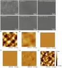
Morphological characterization of AsSe-free Si–Te–Ge chalcogenide glass thin films. (a)–(e) Top-view FESEM images of STG-0 to STG-4 films. (f)–(j) Corresponding AFM height maps (2 × 2 μm2).
AFM measurements were employed to quantitatively assess surface roughness and nanoscale topography (Figure 2(f)−(j)). Representative AFM height maps (2 × 2 μm2 scan area) show that all films possess extremely smooth surfaces, with root-mean-square (RMS) roughness values below 0.5 nm. Among the series, the balanced STG-2 (Si10Ge10Te80) film exhibits the lowest RMS roughness (~0.28 nm), whereas the Ge-rich and Si-rich end members show slightly higher values (~0.35–0.45 nm). The reduced roughness in STG-2 is attributed to optimized network rigidity and homogeneous atomic packing, arising from the cooperative presence of Si and Ge as network formers [33]. Such ultra-smooth surfaces are particularly advantageous for OTS device fabrication, as they minimize local electric-field enhancement at electrode interfaces and reduce the probability of premature breakdown or localized Joule heating during threshold switching.
The morphological homogeneity observed here is directly correlated with the excellent electrical performance of the Si–Te–Ge OTS selectors. In particular, the lack of nanoscale crystalline nuclei or phase-separated regions is crucial for achieving stable and repeatable threshold switching. Local crystallization or density fluctuations can act as preferential conduction pathways, leading to excessive off-state leakage or irreversible filament formation. The superior endurance and low Ioff observed for STG-2 are therefore not only a consequence of its optimized electronic structure but also a reflection of its highly uniform amorphous morphology. By contrast, the reduced endurance of the Si-rich STG-4 sample may be linked to its lower crystallization temperature, which could allow gradual microstructural evolution under repeated electrical stress, even if such changes are not immediately visible in the as-deposited state.
Tauc plot analysis of the UV–Vis absorption data yielded the optical bandgaps listed in Table 2. Notably, the STG-2 sample (balanced Si/Ge) exhibits the largest Eg ≈ 1.05 eV, whereas the extremes have smaller gaps (~0.75–0.80 eV). This mirrors the crystallization temperature trend, suggesting that the widest-gap glass is obtained at intermediate composition. The increase in Eg with Si content is expected due to Si’s lower polarizability; pure a-SiTe has Eg > ~1.0–1.1 eV, whereas pure a-GeTe6 is ~0.6–0.7 eV [34]. Our ternary glasses fall in between. The optical gap is an important indicator because a larger gap generally correlates with lower intrinsic carrier density and thus lower Ioff in OTS off-state.
The refractive index values in Table 2, measured at a telecom wavelength of 1.55 µm, also reflect the composition trends. STG-2 has the lowest index (~2.95), consistent with its higher gap, whereas Ge-rich STG-0 has the highest index (~3.17). Chalcogenide glass refractive indices generally increase with heavier, more polarizable constituents (Ge, Te) and decrease with lighter, more covalent ones (Si) [35]. The static dielectric constants εr follow a similar trend, ranging from ~17 for STG-2 up to ~22 for STG-0. Lower dielectric constant in STG-2 suggests fewer polarizable mid-gap defect states, which correlates with the improved off-state insulation. These compositional tunings of optical/electrical properties highlight how Si and Ge act as complementary modifiers in the Te-based glass: Si raises network connectivity (lowering index and dielectric constant, widening bandgap), whereas Ge increases polarizability and mid-gap state density (raising index and dielectric constant, narrowing gap). The intermediate composition strikes a balance, which, as we will see, translates into superior OTS switching performance.
3.2. Electrical switching performance
We next evaluate the DC and pulsed I–V characteristics of OTS devices made with each glass. All devices exhibit the classic threshold switching behavior: very low current in the off-state until a sudden jump at Vth, followed by a snap-back into a low-voltage high-current on-state. Figure 3(a) compares the DC I–V sweep curves for devices of all five compositions (device diameter = 200 nm). For clarity, Figure 3(b) shows individual I–V curves for each composition on log-linear axes, while Figure 3(c) overlays the post-switch I–V branches of the four Si-containing compositions to visualize differences in holding behavior and off-currents. Several important trends are apparent.
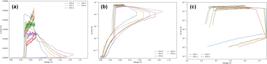
DC I–V characteristics of OTS selector devices with different Si–Ge compositions (device diameter 200 nm). (a) Schematic of the two-probe measurement circuit (1 kΩ series resistor). (b) Log-scale I–V sweeps for each indicated composition, showing volatile threshold switching. (c) Overlay of the I–V curves in the on-state region for four compositions.
First, the threshold voltage systematically depends on composition. Ge-rich STG-0 exhibits the lowest Vth~0.9 V (after the initial forming step), whereas Si-rich STG-4 has the highest Vth ~1.6 V [36]. The mixed compositions lie in between (STG-2 has Vth ~1.2 V). This trend – higher Si content leading to higher Vth – is in line with expectations since adding Si widens the mobility gap and reduces the density of sub-gap states, requiring a stronger electric field to initiate band-tailing impact ionization or trap-filling that triggers threshold switching [37]. Our data quantitatively agree with WU et al.’s [12] report on binary Si–Te: they observed Vth increasing from ~0.9 V to ~1.3 V as Si content increased from 0 to 20 at.%. We similarly see ~0.7 V difference between STG-0 and STG-4. Notably, STG-2’s Vth ≈ 1.2 V is only slightly higher than the Ge-rich glass, suggesting that incorporating 10% Si raises Vth modestly while dramatically improving other aspects as we discuss below.
Second, the off-state leakage current (Ioff) – measured at half of each device’s Vth – shows a steep drop as Si content increases. From Figure 3(c) and Table 3, STG-0 (Ge20Te80) has Ioff ≈ 1.1 × 10⁻⁷ A at ~0.46–0.50 V (Vth/2, with Vth ≈ 0.92 V), whereas STG-4 (Si20Te80) has Ioff ≈ 1.5 × 10⁻⁷ A at ~ 0.79–0.80 V (Vth/2, with Vth ≈ 1.58 V). For an additional cross-composition comparison at the same read bias, we also extracted I (V = 0.5 V); as expected for the OFF-state regime, the leakage at 0.5 V is lower than at ~0.8 V for STG-4 (on the order of 10–8 A or below), while STG-0 remains around 10–7 A at 0.5 V. This confirms that Si incorporation suppresses leakage under equal-bias read conditions, consistent with the half-bias/nonlinearity criteria commonly used for OTS selector evaluation. Thus, a ~20× reduction in leakage was achieved by replacing Ge with Si [38]. Even after normalizing for the slightly different bias (since half of a larger Vth is used for each), the trend holds – e.g., at a common 0.5 V bias, STG-4’s current was ~10–8 A vs. ~10–7 A for STG-0. This can be attributed to the wider bandgap and fewer thermally excited carriers in Si-rich glasses, as well as possibly deeper trap levels that suppress carrier transport in the OFF state [39]. We did notice a slight anomaly for STG-4 in that its leakage was a bit higher than STG-3 (Si15Ge5Te80) under equivalent conditions. This is likely related to STG-4’s lower crystallization stability; as we will discuss in endurance results, the Si-only glass tended to develop higher residual conduction after repeated switching (possibly due to incipient crystallization or filamentary paths forming) [40]. But at fresh state, the overall leakage hierarchy is clear: more Si yields lower Ioff.
Electrical performance metrics of Si–Te–Ge OTS devices (initial fresh-state values for 200 nm cells).
Third, all devices show excellent nonlinearity and selectivity. The current in the on-state at full bias (V = Vth) is on the order of 10–4 A, whereas at half-bias it is ~10–7–10–8 A, giving on/off ratios >103 (in fact ~104 for STG-2 and STG-4). The slope of the I–V in the off regime is very steep, ~12 mV/decade for STG-0 and ~8 mV/dec for STG-4, indicating abrupt threshold switching. These values are comparable to the best OTS selectors reported (typically 5–50 mV/dec) [41]. We note that no threshold switching was observed in control devices made with a non-OTS insulating film (e.g. SiO2 of similar thickness), confirming that the observed nonlinear switching is indeed a bulk property of the chalcogenide material.
Finally, the holding voltage (Vhold) – the voltage to which the device snaps back after threshold switching – did not vary strongly with composition. In all cases Vhold was ~0.3–0.4 V, consistent with chalcogenide OTS behavior being governed by a generic carrier generation process that, once triggered, sustains conduction until a universal low-field conduction regime is reached [42]. The similarity of Vhold (~0.3 V) across our samples suggests that the hold regime is dominated by extended-state conduction in Te, which is common to all, whereas Vth differences arise from differing defect levels and trap distributions introduced by Si vs Ge.
From Table 3, one can see that our AsSe-free Si–Te–Ge selectors compare favorably to other reported Te-based OTS selectors [1]. For instance, STG-2 achieves a selectivity of ~6.6 × 10³ and endurance 108 cycles, which is on par with or better than many As-containing selectors (which typically range 103–104 selectivity and 106 > –109 cycles) [43]. The threshold voltage ~1.25 V is moderate, well below the ~3 V of GeS-based selectors but slightly above the ~0.9 V of some As–Se selectors [44]. Most importantly, the off-current ~5 × 10⁻⁸ A is extremely low – in the 10 nA range – meeting the requirement for large arrays. This low Ioff is comparable to the best achieved by more exotic selectors (e.g. ~10 nA in C–Te or N-doped GeSe) [36]. The STG-4 composition (Si-only) did have even lower fresh Ioff, but its endurance was poor (105 cycles). In fact, cycling tests (discussed next) reveal that STG-2 is the optimum when considering overall performance balance.
3.3. Endurance and switching speed
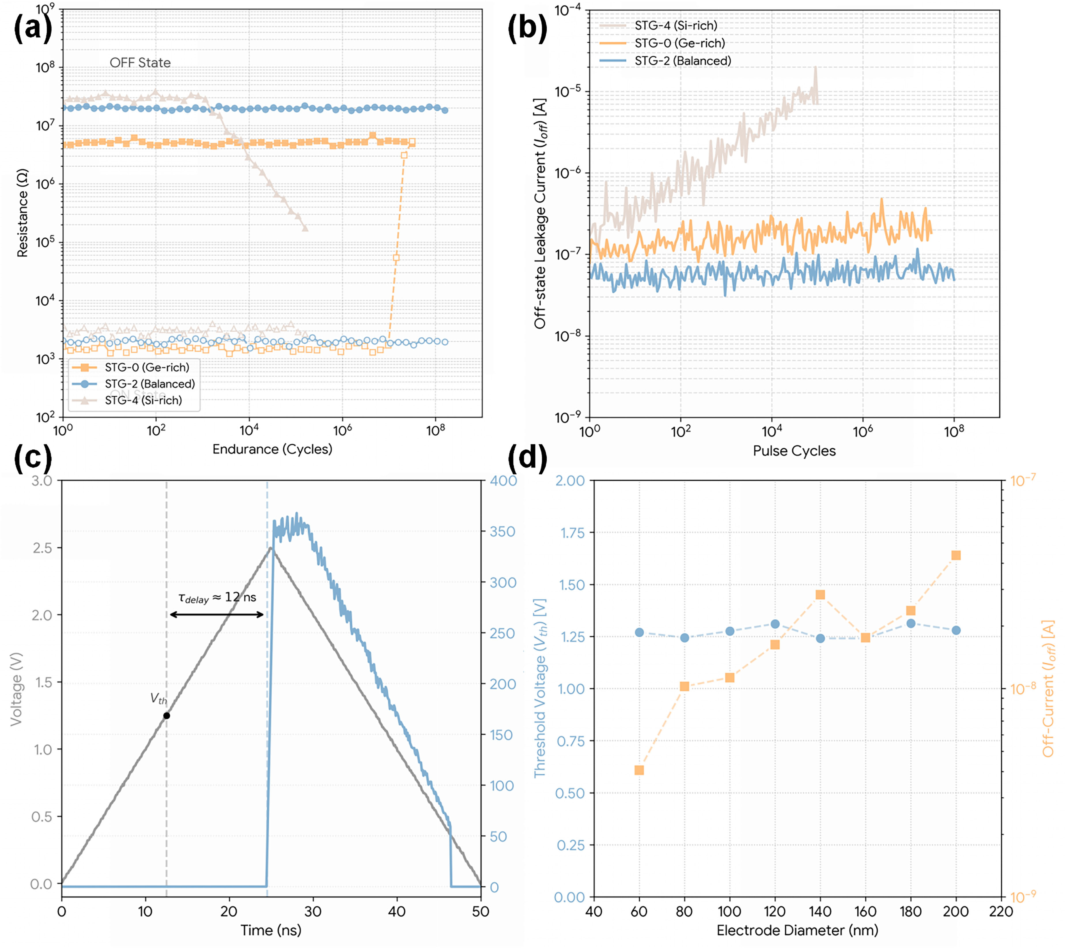
We measured the endurance (repetitive switching cycling) of devices under pulsed bias to evaluate the reliability of the Si–Te–Ge selectors. The criterion for failure was defined as either the selector failing to switch (remaining in a high-resistive state) or its off-current increasing by >10 times (indicating permanent damage or crystallization). Figure 4(a) presents the endurance characteristics for the representative compositions. The results show a stark contrast: the balanced STG-2 device endured >108 set/reset cycles without failure, maintaining a stable resistance window throughout the test. In comparison, the Si-rich STG-4 failed significantly earlier, after approximately 105 cycles, while the Ge-rich STG-0 failed after ~3 × 10⁷ cycles.
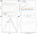
Dynamic performance and scalability of Si–Te–Ge OTS selectors. (a) Endurance cycling characteristics of STG-0, STG-2, and STG-4 devices. (b) Evolution of the off-state leakage current (Ioff) versus cycle number. (c) Typical transient switching waveforms (Voltage vs. Time and Current vs. Time) for an STG-2 device. (d) Scalability analysis showing the threshold voltage (Vth) and off-current (Ioff) as a function of bottom electrode diameter (60 nm to 200 nm) for the STG-2 composition.
The failure mechanisms differ distinctly between the compositions. As detailed in Figure 4(b), which tracks the evolution of the off-state leakage current (Ioff) during cycling, STG-4 exhibits a gradual but continuous increase in leakage. After 105 cycles, its Ioff rose by approximately two orders of magnitude (reaching ~10-5 A), leading to a loss of selectivity. This behavior is consistent with partial crystallization of the Si–Te film over time, as its low Tx (~130 °C) likely allowed cumulative Joule heating to induce crystal nuclei formation. In contrast, STG-2 showed negligible Ioff drift up to 108 cycles, validating that the higher crystallization barrier (Tx = 235 °C) effectively suppresses devitrification under thermal stress. Meanwhile, STG-0 typically failed via a “stuck-off” mode, attributed to gradual structural relaxation or void formation typical of Ge-rich chalcogenides.
Switching speed measurements were conducted by applying fast triangular voltage pulses and capturing the time-resolved current response. Figure 4(c) displays the typical transient switching waveforms for an STG-2 device. All compositions demonstrated ultra-fast threshold switching, with a characteristic delay time (τdelay) on the order of 10–20 ns and a recovery time of ~100 ns. We did not observe a significant dependence of the switching speed on the Si/Ge ratio; the transition times remained clustered around 10 ns across the series. This implies that the fundamental switching mechanism operates on similar time scales for these Te-based glasses regardless of the specific dopant ratio.
Finally, the scalability of the selector was confirmed. Figure 4(d) summarizes the dependence of threshold voltage (Vth) and off-current Ioff on device electrode diameter ranging from 200 nm down to 60 nm. The devices functioned with consistent Vth and stable leakage density across all dimensions, indicating excellent film uniformity and the absence of strong size effects or perimeter-dominated leakage pathways. These results confirm that the optimized STG-2 composition is suitable for high-speed, high-density memory arrays.
3.4. ML interpretation of composition–property relationships
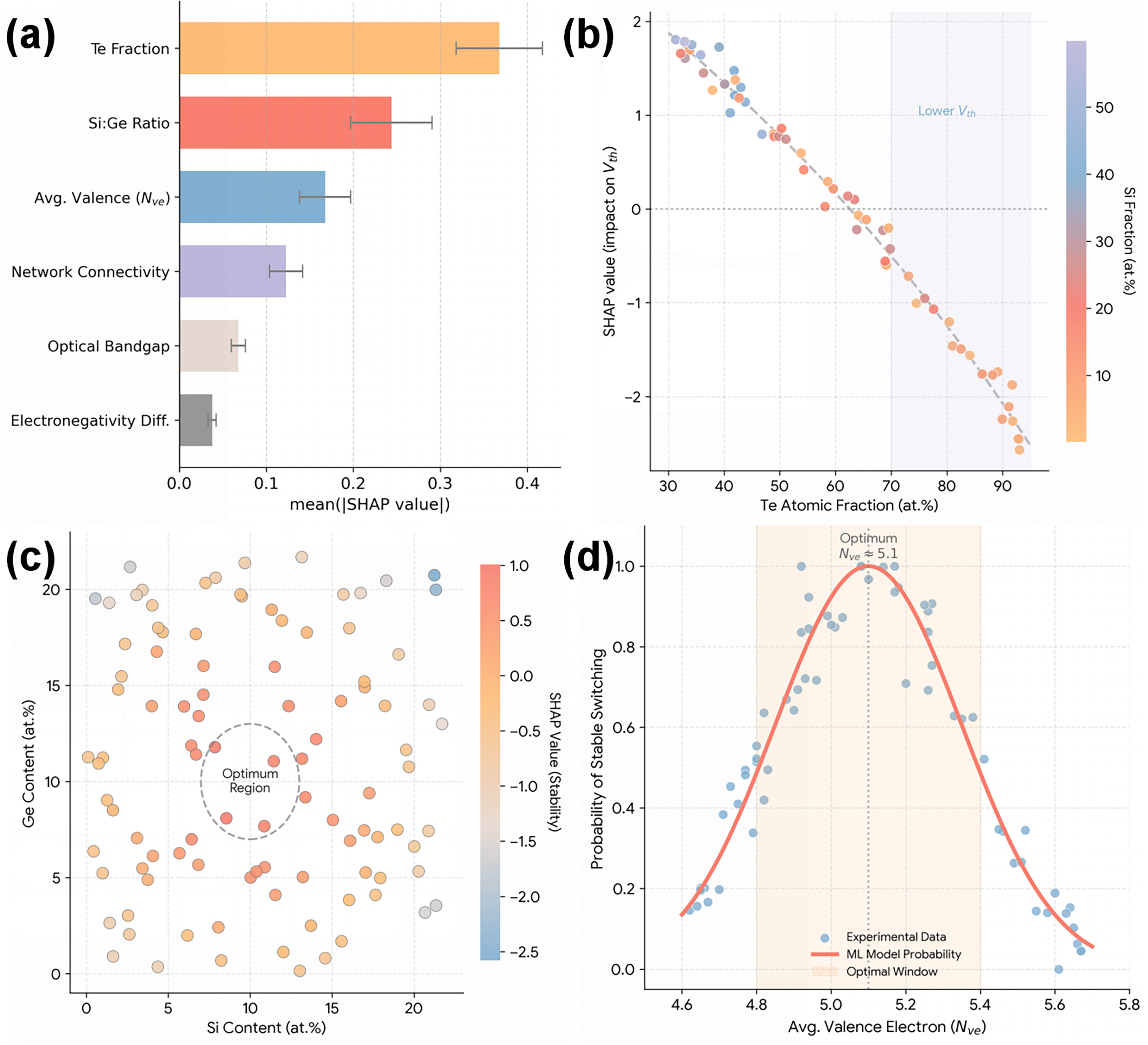
To understand why the STG-2 composition is optimal and to guide future materials design, we turn to the interpretable ML model described earlier. The results of this analysis are summarized in Figure 5.
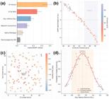
Interpretable machine learning analysis of OTS material properties. (a) Global feature importance ranking extracted from the gradient-boosted decision tree model. (b) SHAP dependence plot for Te atomic fraction. (c) Two-variable interaction map. (d) Probability distribution of stable OTS switching behavior as a function of average valence electron number (Nve).
First, we examine the global drivers of selector performance. As shown in Figure 5(a), the ML model ranked the features by their overall impact on the predictions. The top factors identified were: (1) Te fraction, which dominates the conductive properties; (2) Si:Ge ratio, which governs the stability/leakage trade-off; (3) Average valence electron number (Nve); and (4) Network connectivity. This ranking provides a rational basis for our design: Te fraction controls the ease of carrier generation, while the Si:Ge ratio and Nve determine the trap depth and structural rigidity required to maintain the amorphous state under stress.
To understand how these top features specifically influence the material properties, we analyze the SHAP dependence plots shown in Figure 5(b)–(d):
-
Te content (Figure 5(b)): The model indicated that higher Te content (and hence lower average bond energy) tends to lower Vth but increase Ioff, in agreement with our experimental observation that Ge-rich (more Te relative to network formers) yields lowest Vth but highest leakage. The SHAP analysis in Figure 5(b) confirms this trend: compositions with Te rising above ~70% are predicted to have easier threshold switching (lower Vth) but suffer from worse off-state holding capability5. This matches the known role of Te in providing heavy polarizable orbitals that facilitate conduction.
-
Si vs Ge balance (Figure 5(c)): The model captured that Si and Ge play complementary roles. Increasing Si raises the glass’s bandgap and trap depth, strongly reducing Ioff, but excessive Si can reduce mean coordination compared to Ge, potentially affecting stability. The SHAP “interaction” map in Figure 5(c) reveals that an intermediate mix of Si and Ge maximizes the predicted stability index. In essence, the model supports that a dual-network-former glass (combining tetrahedral Si with the slightly more flexible Ge coordination) yields a network that is both robust and not overly constrained. This aligns with our experimental Tx peaking at the intermediate STG-2 composition.
-
Average coordination/Nve (Figure 5(d)): All our compositions possess an Nve of ~5.1, which falls within the ideal range for OTS materials. The ML model confirms this in Figure 5(d), showing that if Nve strays far from 5 (e.g., >5.5 or <4.7), the probability of stable OTS behavior diminishes. Our As/Se-free system allows Nve tuning via composition to stay within this optimal window, confirming that the Ovshinsky rule remains a guiding principle even without As or Se.
-
Trap density and bandgap: Finally, using proxies like optical gap and polarizability, the model indicated that a moderate optical gap (~1 eV) is optimal. A gap that is too low (e.g., 0.6 eV) leads to semiconductor-like excessive leakage, whereas a gap that is too high (>1.5 eV) behaves like an insulator, preventing switching. Our STG-2’s gap of ~1.05 eV falls precisely in the “sweet spot” predicted, distinguishing it from the binary extremes.
In light of these insights, the success of the STG-2 composition becomes clear. It has ~80% Te to enable threshold switching, yet the remaining 20% is split evenly between Si and Ge. This split creates a rigid, high-Tg network that prevents crystallization without introducing deep traps that would require an excessively high field. The ML model correctly flags this composition as the optimal compromise, a finding validated by our experimental results.
Furthermore, the interpretable nature of this analysis gives confidence that other AsSe-free systems can be engineered similarly. For instance, adding light elements (like C or B) to increase average coordination could further lower Ioff, though likely at the cost of higher Vth—trade-offs that the model can now quantitatively evaluate [23].
Regarding the switching mechanism, the evidence of symmetrical I–V behavior and Poole-Frenkel conduction fits (trap depths ~0.3–0.4 eV) points to a conventional thermal/electronic positive feedback mechanism common in amorphous chalcogenides. Unlike pure crystalline Te devices, our Si–Te–Ge glasses operate in the amorphous state. Si does not introduce a new mechanism but rather modifies the defect populations that form the conductive path.
4. CONCLUSION
In this work, we developed and characterized an arsenic- and selenium-free Si–Te–Ge chalcogenide glass for use as an ovonic threshold switching (OTS) selector in memory applications. By synergistically combining experimental materials science with interpretable machine learning, we identified an optimal ternary composition (~10 at.% Si, 10 at.% Ge, 80 at.% Te) that achieves an excellent balance of low leakage current, moderate switching voltage, and high thermal stability. Comprehensive material characterization confirmed that all Si–Te–Ge films are fully amorphous and homogeneous, with the incorporation of Si significantly increasing the glass transition and crystallization temperatures and widening the bandgap relative to Ge–Te binary analogues. OTS devices fabricated with these glasses exhibit volatile threshold switching with high non-linearity (on/off ratios >103–104) and fast switching speed (~10 ns). Critically, replacing As/Se with Si/Ge did not degrade performance – in fact, the optimized Si–Ge–Te device showed ultra-low off-state leakage (~5 × 10⁻⁸ A) and sustained over 108 switching cycles without failure, outperforming many legacy As/Se-based selectors in endurance and leakage suppression. The only trade-off was a modest increase in threshold voltage (1.2–1.3 V, as opposed to ~0.9 V in some As-based systems), which remains within acceptable limits for circuit operation.
Our interpretable ML analysis provided valuable insights into the composition–property relationships governing OTS behavior. The models highlighted that Te content, average valence electron count, and network connectivity are key predictors of threshold switching performance. In essence, Te-rich networks are needed for easy switching, but the network must be sufficiently rigid (via Si, Ge) to avoid crystallization and minimize leakage. These principles guided us to the Si–Te–Ge solution presented. The success of this AsSe-free OTS selector is significant for practical applications, as it eliminates toxic elements while delivering state-of-the-art selector metrics. Our findings also underscore the effectiveness of combining machine learning with materials experimentation to accelerate discovery: the ML model helped narrow down the vast compositional space to a few promising candidates, and its interpretability ensured the design choices were grounded in physical reasoning. Future work may explore doping the Si–Ge–Te glass with small amounts of other elements to further tailor its properties, with the framework established here serving as a guide. We believe the AsSe-free Si–Te–Ge OTS selector reported here is a strong candidate for next-generation high-density memory selectors, combining environmental safety with high performance and reliability, and represents a step forward in the rational design of functional amorphous materials.
5. ACKNOWLEDGMENTS
This work has been supported by Henan Provincial Key R&D Program: Research on Key Technologies for Large-Scale Warehouse Logistics Based on Deep Learning (251111211500) and Research on Key Technologies for Field Identification and Classification of Medicinal Plants Using UAV Hyperspectral Imaging. This research was funded in part by the Key Research Projects of Henan Science and Technology Department under Grant 262102311248.
6. BIBLIOGRAPHY
-
[1] ZHAO, Z., CLIMA, S., GARBIN, D., et al., “Chalcogenide ovonic threshold switching selector”, Nano- Micro Letters, v. 16, n. 1, pp. 81, Jan. 2024. doi: https://doi.org/10.1007/s40820-023-01289-x. PubMed PMID: 38206440.
» https://doi.org/10.1007/s40820-023-01289-x -
[2] HODDESON, L., GARRETT, P., “The discovery of Ovshinsky switching and phase-change memory”, Physics Today, v. 71, n. 6, pp. 44–51, 2018. doi: https://doi.org/10.1063/PT.3.3948.
» https://doi.org/10.1063/PT.3.3948 -
[3] ZHAO, Z., CLIMA, S., GARBIN, D., et al., “Chalcogenide ovonic threshold switching selector”, Nano-Micro Letters, v. 16, n. 1, pp. 81, Jan. 2024. doi: https://doi.org/10.1007/s40820-023-01289-x. PubMed PMID: 38206440.
» https://doi.org/10.1007/s40820-023-01289-x -
[4] VELEA, A., OPSOMER, K., DEVULDER, W., et al., “Te-based chalcogenide materials for selector applications”, Scientific Reports, v. 7, n. 1, pp. 8103, Aug. 2017. doi: https://doi.org/10.1038/s41598-017-08251-z. PubMed PMID: 28808294.
» https://doi.org/10.1038/s41598-017-08251-z -
[5] LEE, M., LEE, S., KIM, M., et al., “Ge1−xSx chalcogenide alloys for OTS applications using magnetron sputtering”, Journal of Alloys and Compounds, v. 930, pp. 167409, Jan. 2023. doi: https://doi.org/10.1016/j.jallcom.2022.167409.
» https://doi.org/10.1016/j.jallcom.2022.167409 -
[6] WANG, Y., WANG, H., FU, X., et al., “Optimal stoichiometry and performance evolution in As-Se based OTS devices”, Materials Science in Semiconductor Processing, v. 202, pp. 110079, Feb. 2026. doi: https://doi.org/10.1016/j.mssp.2025.110079.
» https://doi.org/10.1016/j.mssp.2025.110079 -
[7] KOLOBOV, A.V., KUZNETSOV, V.G., KRBAL, M., et al., “Lone-pair-enabled polymorphism and photostructural changes in chalcogenide glasses”, Materials, v. 16, n. 19, pp. 6602, Oct. 2023. doi: https://doi.org/10.3390/ma16196602. PubMed PMID: 37834739.
» https://doi.org/10.3390/ma16196602 -
[8] NOÉ, P., VERDY, A., d’Acapito, F., et al., “Toward ultimate nonvolatile resistive memories: the mechanism behind ovonic threshold switching revealed”, Science Advances, v. 6, n. 9, eaay2830, Feb. 2020. doi: https://doi.org/10.1126/sciadv.aay2830. PubMed PMID: 32158940.
» https://doi.org/10.1126/sciadv.aay2830 -
[9] LI, Y., WANG, H., SHAO, M., et al., “Modulation of GeSe and As2Se3 motifs to optimise GeAsSe OTS performance and its mechanism”, Journal of Materials Chemistry. C, Materials for Optical and Electronic Devices, v. 13, n. 2, pp. 735–742, Jan. 2025. doi: https://doi.org/10.1039/D4TC03586K.
» https://doi.org/10.1039/D4TC03586K -
[10] SAJITHA, D.R., STEPHEN, B., NAKAMURA, A., et al., “The emergence of chalcogenides: A new era for thin film solar absorbers”, Progress in Solid State Chemistry, v. 76, pp. 100490, Dec. 2024. doi: https://doi.org/10.1016/j.progsolidstchem.2024.100490.
» https://doi.org/10.1016/j.progsolidstchem.2024.100490 -
[11] YANG, Y., WU, K., ZHANG, B., et al., “Infrared nonlinear optical polymorphs α- and β-SrCu2SnS4 exhibiting large second harmonic generation responses with requisite phase-matching behavior”, Chemistry of Materials, v. 32, n. 3, pp. 1281–1287, Feb. 2020. doi: https://doi.org/10.1021/acs.chemmater.9b04842.
» https://doi.org/10.1021/acs.chemmater.9b04842 -
[12] WU, R., SUN, Y., ZHANG, S., et al., “Great potential of Si-Te ovonic threshold selector in electrical performance and scalability”, Nanomaterials, v. 13, n. 6, pp. 1114, Jan. 2023. doi: https://doi.org/10.3390/nano13061114. PubMed PMID: 36986008.
» https://doi.org/10.3390/nano13061114 -
[13] KARAKSINA, E.V., BLAGIN, R.D., SUKHANOV, M.V., et al., “Preparation and properties of especially pure Ge-Sb-As-S glasses for IR optics”, Journal of Non-Crystalline Solids, v. 642, pp. 123158, Oct. 2024. doi: https://doi.org/10.1016/j.jnoncrysol.2024.123158.
» https://doi.org/10.1016/j.jnoncrysol.2024.123158 -
[14] WU, R., JIA, S., GOTOH, T., et al., “Screening switching materials with low leakage current and high thermal stability for neuromorphic computing”, Advanced Electronic Materials, v. 8, n. 9, pp. 2200150, 2022. doi: https://doi.org/10.1002/aelm.202200150.
» https://doi.org/10.1002/aelm.202200150 -
[15] YIMAM, D.T., VAN DER REE, A.J.T., ABOU EL KHEIR, O., et al., “Phase separation in Ge-Rich GeSbTe at different length scales: melt-quenched bulk versus annealed thin films”, Nanomaterials, v. 12, n. 10, pp. 1717, May. 2022. doi: https://doi.org/10.3390/nano12101717. PubMed PMID: 35630939.
» https://doi.org/10.3390/nano12101717 -
[16] XIAO, F., LIN, W., CHENG, Q., “Ab-initio calculations and molecular dynamics simulations of In, Ag, and Cu replacing Zn in sphalerite: implications for critical metal mineralization”, Ore Geology Reviews, v. 163, pp. 105699, Dec. 2023. doi: https://doi.org/10.1016/j.oregeorev.2023.105699.
» https://doi.org/10.1016/j.oregeorev.2023.105699 -
[17] QIAO, C., XU, M., WANG, S., et al., “Structure, bonding nature and transition dynamics of amorphous Te”, Scripta Materialia, v. 202, pp. 114011, Sep. 2021. doi: https://doi.org/10.1016/j.scriptamat.2021.114011.
» https://doi.org/10.1016/j.scriptamat.2021.114011 -
[18] VELEA, A., OPSOMER, K., DEVULDER, W., et al., “Te-based chalcogenide materials for selector applications”, Scientific Reports, v. 7, n. 1, pp. 8103, Aug. 2017. doi: https://doi.org/10.1038/s41598-017-08251-z. PubMed PMID: 28808294.
» https://doi.org/10.1038/s41598-017-08251-z -
[19] CHAHAL, S., RAMESH, K., “Glass formation, thermal stability and fragility minimum in Ge-Te-Se glasses”, Materials Research Bulletin, v. 152, pp. 111833, Aug. 2022. doi: https://doi.org/10.1016/j.materresbull.2022.111833.
» https://doi.org/10.1016/j.materresbull.2022.111833 -
[20] SANKARAPANDIAN, K., ALSHAHRANI, H.M., ALOTAIBI, F.A., et al., “Estimating punching performance in fiber-reinforced polymer concrete slabs utilizing machine learning and gradient-boosted regression techniques”, Matéria (Rio de Janeiro), v. 30, e20240668, 2025. doi: https://doi.org/10.1590/1517-7076-rmat-2024-0668.
» https://doi.org/10.1590/1517-7076-rmat-2024-0668 -
[21] MAZROA, A.A., ALOTAIBI, F.A., ALNFIAI, M.M., et al., “Predicting bond strength between steel reinforcement and concrete materials using machine learning with Bayesian optimization techniques”, Matéria, v. 30, e20240740, 2025. doi: https://doi.org/10.1590/1517-7076-rmat-2024-0740.
» https://doi.org/10.1590/1517-7076-rmat-2024-0740 -
[22] GARBIN, D., et al., “Composition optimization and device understanding of Si-Ge-As-Te Ovonic threshold switch selector with excellent endurance”, In: Proceedings of the 2019 IEEE International Electron Devices Meeting (IEDM), pp. 35.1.1-35.1.4, Dec. 2019. doi: https://doi.org/10.1109/IEDM19573.2019.8993547.
» https://doi.org/10.1109/IEDM19573.2019.8993547 -
[23] ZAKI, M., JAYADEVA, KRISHNAN, N.M.A., “Interpretable machine learning for understanding compositional and testing condition effects on refractive index, density, dielectric constant, and loss tangent of inorganic melts and glasses’”, Frontiers in Materials, v. 11, pp. 1412701, Sep. 2024. doi: https://doi.org/10.3389/fmats.2024.1412701.
» https://doi.org/10.3389/fmats.2024.1412701 -
[24] BOUŠKA, M., NAZABAL, V., GUTWIRTH, J., et al., “Radio-frequency magnetron co-sputtered Ge-Sb-Te phase change thin films”, Journal of Non-Crystalline Solids, v. 569, pp. 121003, Oct. 2021. doi: https://doi.org/10.1016/j.jnoncrysol.2021.121003.
» https://doi.org/10.1016/j.jnoncrysol.2021.121003 -
[25] KARKI, V., DEBNATH, A.K., KUMAR, S., et al., “Synthesis of co-sputter deposited Ni–Ti thin alloy films and their compositional characterization using depth sensitive techniques”, Thin Solid Films, v. 697, pp. 137800, Mar. 2020. doi: https://doi.org/10.1016/j.tsf.2020.137800.
» https://doi.org/10.1016/j.tsf.2020.137800 -
[26] OKE, J.A., OLOTU, O.O., JEN, T.-C., “Atomic layer deposition of chalcogenide thin films: processes, film properties, applications, and bibliometric prospect”, Journal of Materials Research and Technology, v. 20, pp. 991–1019, Sep. 2022. doi: https://doi.org/10.1016/j.jmrt.2022.07.098.
» https://doi.org/10.1016/j.jmrt.2022.07.098 -
[27] DU, X., XU, H., ZHU, F., “Understanding the effect of hyperparameter optimization on machine learning models for structure design problems”, Computer Aided Design, v. 135, pp. 103013, Jun. 2021. doi: https://doi.org/10.1016/j.cad.2021.103013.
» https://doi.org/10.1016/j.cad.2021.103013 -
[28] BORGES, P.P.P.O., RITCHIE, R.O., ASTA, M., “Local lattice distortions and the structural instabilities in bcc Nb–Ta–Ti–Hf high-entropy alloys: an ab initio computational study”, Acta Materialia, v. 262, pp. 119415, Jan. 2024. doi: https://doi.org/10.1016/j.actamat.2023.119415.
» https://doi.org/10.1016/j.actamat.2023.119415 -
[29] CIOBANU, M., GALCA, A.C., SAVA, F., et al., “First Sharp Diffraction Peak features of the intermediate phase glasses and amorphous thin films in the non-stoichiometric (GeS4)x(AsS3)1-x system”, Thin Solid Films, v. 773, pp. 139828, May. 2023. doi: https://doi.org/10.1016/j.tsf.2023.139828.
» https://doi.org/10.1016/j.tsf.2023.139828 -
[30] PRAZAKOVA, L., NOLOT, E., MARTINEZ, E., et al., “The effect of Ge content on structural evolution of Ge-rich GeSbTe alloys at increasing temperature”, Materialia, v. 21, pp. 101345, Mar. 2022. doi: https://doi.org/10.1016/j.mtla.2022.101345.
» https://doi.org/10.1016/j.mtla.2022.101345 -
[31] YUAN, R., GUO, Y., GURGAN, I., et al., “Raman spectroscopy analysis of disordered and amorphous carbon materials: a review of empirical correlations”, Carbon, v. 238, pp. 120214, May. 2025. doi: https://doi.org/10.1016/j.carbon.2025.120214.
» https://doi.org/10.1016/j.carbon.2025.120214 -
[32] DEVULAPALLI, V., HANS, M., SUKUMAR, P.T., et al., “Microstructure, grain boundary evolution and anisotropic Fe segregation in (0001) textured Ti thin films”, Acta Materialia, v. 238, pp. 118180, Oct. 2022. doi: https://doi.org/10.1016/j.actamat.2022.118180.
» https://doi.org/10.1016/j.actamat.2022.118180 -
[33] GERRITSEN, S.H., CHITTOCK, N.J., VANDALON, V., et al., “Surface smoothing by atomic layer deposition and etching for the fabrication of nanodevices”, ACS Applied Nano Materials, v. 5, n. 12, pp. 18116–18126, Dec. 2022. doi: https://doi.org/10.1021/acsanm.2c04025. PubMed PMID: 36583128.
» https://doi.org/10.1021/acsanm.2c04025 -
[34] WINTERSTELLER, S., YAREMA, O., KUMAAR, D., et al., “Unravelling the amorphous structure and crystallization mechanism of GeTe phase change memory materials”, Nature Communications, v. 15, n. 1, pp. 1011, Feb. 2024. doi: https://doi.org/10.1038/s41467-024-45327-7. PubMed PMID: 38307863.
» https://doi.org/10.1038/s41467-024-45327-7 -
[35] FAN, P., GAO, C., ZHOU, G., et al., “Large-scale As-Sb-S chalcogenide glasses with ultrahigh gradient refractive index”, Materials & Design, v. 252, pp. 113815, Apr. 2025. doi: https://doi.org/10.1016/j.matdes.2025.113815.
» https://doi.org/10.1016/j.matdes.2025.113815 -
[36] PARK, S., KIM, M., KIM, T.H., et al., “Thermal atomic layer deposition of ternary Ge-S-Se alloy for advanced ovonic threshold switch selectors in three-dimensional cross-point memory array”, Journal of Alloys and Compounds, v. 968, pp. 172284, Dec. 2023. doi: https://doi.org/10.1016/j.jallcom.2023.172284.
» https://doi.org/10.1016/j.jallcom.2023.172284 -
[37] XIE, D., HEIMLER, P., BOLDYRJEW-MAST, R., et al., “Threshold voltage hysteresis investigation of SiC MOSFETs with different structures under various measurement conditions”, Microelectronics and Reliability, v. 168, pp. 115657, May. 2025. doi: https://doi.org/10.1016/j.microrel.2025.115657.
» https://doi.org/10.1016/j.microrel.2025.115657 -
[38] GEORGE, A., SUSHAMMA, D., PREDEEP, P., et al., “A study of thermal stability and electrical switching behaviour of Ge–Te–In chalcogenide glass system”, Indian Journal of Physics and Proceedings of the Indian Association for the Cultivation of Science, v. 91, n. 9, pp. 1013–1020, Sep. 2017. doi: https://doi.org/10.1007/s12648-017-0985-3.
» https://doi.org/10.1007/s12648-017-0985-3 -
[39] ASESH, A., “Normalization and bias in time series data”, In: Biele, C., Kacprzyk, J., Kopeć, W. et al. (eds), Digital interaction and machine intelligence, Cham, Springer, pp. 88-97, 2022. doi: https://doi.org/10.1007/978-3-031-11432-8_8.
» https://doi.org/10.1007/978-3-031-11432-8_8 -
[40] ALHALAWEH, A., ALZGHOUL, A., MAHLIN, D., et al., “Physical stability of drugs after storage above and below the glass transition temperature: Relationship to glass-forming ability”, International Journal of Pharmaceutics, v. 495, n. 1, pp. 312–317, Nov. 2015. doi: https://doi.org/10.1016/j.ijpharm.2015.08.101. PubMed PMID: 26341321.
» https://doi.org/10.1016/j.ijpharm.2015.08.101 -
[41] CHEN, C., CAI, Y., SUN, P., et al., “Threshold voltage instability of SiC MOSFETs under very-high temperature and wide gate bias”, IET Power Electronics, v. 17, n. 15, pp. 2393–2404, 2024. doi: https://doi.org/10.1049/pel2.12786.
» https://doi.org/10.1049/pel2.12786 -
[42] SUNG, H.-J., CHOI, M., WU, Z., et al., “Microscopic origin of polarity-dependent VTH Shift in amorphous chalcogenides for 3D self-selecting memory”, Advanced Science, v. 11, n. 44, e2408028, 2024. doi: https://doi.org/10.1002/advs.202408028. PubMed PMID: 39382149.
» https://doi.org/10.1002/advs.202408028 -
[43] WANG, C., YANG, B., GU, Q., et al., “Near 100% ethene selectivity achieved by tailoring dual active sites to isolate dehydrogenation and oxidation”, Nature Communications, v. 12, n. 1, pp. 5447, Sep. 2021. doi: https://doi.org/10.1038/s41467-021-25782-2. PubMed PMID: 34521830.
» https://doi.org/10.1038/s41467-021-25782-2 -
[44] NIROSHA, R., AGARWAL, R., “Characterization and modeling of threshold voltage for organic and amorphous thin-film transistors”, Microelectronics and Reliability, v. 147, pp. 115054, Aug. 2023. doi: https://doi.org/10.1016/j.microrel.2023.115054.
» https://doi.org/10.1016/j.microrel.2023.115054