High Sensitivity Optical Sensor Based on Surface Plasmon Effect on Graphene for Detection of DMSO Concentrations
Abstract
In this study, a rib waveguide is used in the design of a plasmonic sensor. The structure consists of a dielectric substrate constituted of tantalum pentoxide (Ta2O5). On top of this substrate, a superstrate with a ridge, composed of niobium pentoxide (Nb2O5), is overlayed forming the guiding region. A thin sheet of graphene is placed over the Nb2O5 and below the analysis region, where concentrations of dimethyl sulfoxide (DMSO) ranging from 50% to 100% will be detected. The purpose of incorporating the graphene sheet is to induce the effect of localized surface plasmon resonance (LSPR), which in this configuration becomes sensitive to variations in the refractive index (RI) of DMSO. The surface plasmons in graphene (graphene-SP) are induced by collective oscillations of charge carriers, i.e., free electrons in graphene, which, when subjected to specific frequencies, couple with the electromagnetic fields at the interface between graphene and the dielectric. The basic principle is similar to that of surface plasmons in noble metals,however, surface plasmons in graphene can occur at lower frequencies. With this configuration, a plasmonic sensor is obtained to detect DMSO concentrations, designed for a wavelength of 0.6329 micrometers.
Index Terms
DMSO; graphene optical sensor; rib waveguide; surface plasmons.
I. INTRODUCTION
Waveguides are structures capable of confining electromagnetic fields through appropriate boundary conditions, guiding them in a preferred direction of propagation. A rib waveguide is a unique type of device in which the guiding region is formed by a ridge on which one or more dielectric layers are deposited on top of the substrate. The layers of materials within the guiding region are chosen to adjust the effective refractive index (neff) of the structure. These waveguides typically operate by confining optical energy within the guiding region, thus preventing the scattering of the optical field [1]. The rib waveguide offers some advantages over optical fibers in SPR sensor applications, specially related to fabrication [2], [3]. It can be constructed on a dielectric substrate, which improves the integration with electronic and optoelectronic circuits, while also providing enhanced stability and mechanical robustness when interfacing with external systems [4]. In recent years, a single rib waveguide and rib waveguide arrays applied on SPR sensors are widely used in bio-sensing and biochemical sensing for its unique capacity of sensing very small changes in refractive index, therefore, the analyzed model can be applied in various types of optical devices. In [4], a rib waveguide was used in a integrated opto-mechanical cantilever sensor to obtain a improvement of the coupling efficiency in the interface. A multiplexed biosensor based on surface corrugated Bragg gratings on a Rib waveguide structure was proposed in [5], it was reported that the sensor has shown a good sensitivity along the multiplexed sensing. The rib waveguide was used as photodetectors in [6], in this paper the spectral response of the sensor has shown a positive result for integration on all-in-one platform for small-size devices. A hybrid plasmonic waveguide was designed in [7], and its optical power transmission was analyzed. In addition to being electromagnetically compatible with different optical structures, this type of waveguide can be adapted for usage in sensors that exploit the phenomenon of surface plasmon resonance (SPR).
Furthermore, when applied at frequencies where noble metals are typically employed, alternative materials, such as graphene, can be used in its manufacture. Graphene is material used in nanotechnology, composed of sp2 electronic level carbon atoms in a two-dimensional metallic lattice structure [8]. According to the application and excitation wavelength, graphene can exhibit excellent conductivity characteristics [9], [10]. Composed of carbon atoms arranged in a single-layered, flat sheet, the material is one of the crystalline forms of carbon [8]. In recent years, new solutions have been proposed for the usage of graphene in high-frequency applications [9] particularly with the possibility of obtaining thin graphene films through scalable methods, offering an excellent alternative for integration with photonic devices [11]. The electronic structure of graphene enables surface plasmons to occur in the region of the visible spectrum, in contrast to surface plasmons in noble metals, which are generally found in infrared (λ ≥ 0.7 µm).
In this work, a wavelength of 0.6329 µm was used, this parameter will allow the structure proposed in this work to be applied to detect various dimethyl sulfoxide (DMSO) concentrations when the entire structure is excited at optical frequencies, especially at the wavelength of 0.6329 micrometers, coupled to He-Ne (helium-neon) laser beams circuits that has shown good stability, resolution and reduced costs [12]. When excited at the frequency corresponding to this wavelength, the graphene utilized in this structure exhibits plasmonic characteristics [13], [14]. In this context, surface plasmons in graphene displays much stronger electromagnetic field confinement, offering higher spatial resolution and potentially greater sensitivity for sensing applications [15], [16].
The operation of SPR sensors is based on the behaviour of a dielectric-metal interface excited by a beam light. This interaction will cause oscillations in the charge density along that interface, these are also known as surface plasmon oscillations (SPO), the quantum of these oscillations is refereed as surface plasmon mode (SPM) [17], [18]. Surface plasmons are evanescent waves, that is, the propagated field decays exponentially throughout the propagation. Due to this fact, the analysis of these fields occurs locally, thus justifying the term LSPR. In this scenario, this work proposes the analysis of a plasmonic sensor using a rib waveguide, where a thin graphene multilayer, employed as a plasmonic material, is deposited on the Nb2O5 layer, which represents the guiding region. The interest in utilizing DMSO as an analyte in this study is attributable to its notable chemical, pharmaceutical and medical properties. Among these properties, its ability to combine with different types of acids, carbohydrates, lipids and other substances, without permanently altering the molecular composition significantly. Additionally, DMSO has anti-inflammatory action and acts as an antioxidant, providing effective action in different types of inflammatory conditions, such as rheumatoid arthritis, inflammation in the lumbar spine and joint arthritis [19]-[21]. DMSO Concentrations ranging from 50 to 70% are frequently used to treat the illnesses mentioned above. Consequently, the significance of the sensor designed in this work lies in its capability to detect varying concentrations of DMSO [22], since, for biomedical applications, DMSO is normally diluted. In this work, the levels of DMSO analyzed ranged from 50% to its pure concentration of 100%, with intervals of 10% increments per sample.
II. MATERIALS AND METHODS
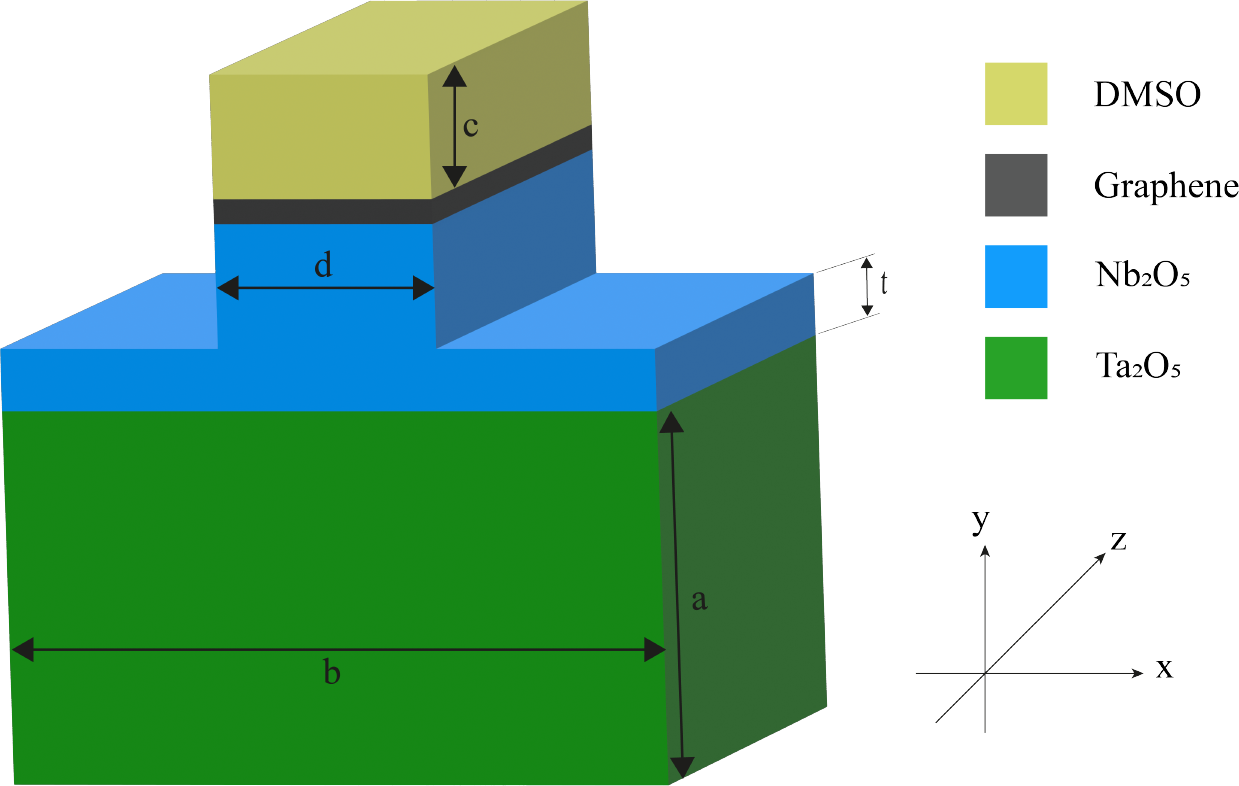
The proposed sensor’s structure consists of a tantalum pentoxide (Ta2O5) substrate, followed by a niobium pentoxide (Nb2O5) layer that forms the signal guiding region. On top of this region is a thin graphene layer, which matches the width of the ridge of the Nb2O5 layer extending along the longitudinal axis, maintaining its dimensions and position unchanged. A micro-channel, of same width, is placed over the graphene layer and contains DMSO samples. For simulation purposes, the structure was immersed in an air box, where perfectly matched layers (PML), layers on which the methods utilized would limit the numerical analysis, were applied to define the computational domain and absorb unwanted evanescent fields. The plasmonic effect, based on the interaction of light with graphene, was investigated through simulations using a original algorithm with a vectorial formulation based on the finite element method (FEM) combined with the vector beam propagation method (VBPM) [22], [23].
Fig. 1 illustrates the proposed structure and the materials used. The waveguide has dimensions: a = 3.5 µm, b = 6 µm, d = 1.4 µm and t = 0.1 µm, the ridge’s micro-channel, where the sample of DMSO is deposited, has a height of c = 0.85 µm. It has been reported in the literature that increasing the layers of graphene can also increase the sensitivity of the sensor [9], [24], [25], even the associations of graphene and other materials, such as gold, has been reported to have a increasing linear sensitivity scaling along the axis with l number of layers, via numerical method predictions [25]. Graphite, being a three-dimensional solid with stacked and strongly coupled π-bonds [26], has different electrical and adsorption properties than graphene and, therefore, a much lower sensitivity [27]. However, the corelation between the number of layers and sensitivity is not always linear and, for the purposes of this report, a limit of layers was employed to balance the sensor’s performance to match the application. The graphene layer has a thickness of 0.014 µm, resulting in 20 stacked layers of graphene to guarantee the balance between sensibility and propagation distance. It is also important to emphasize that doping capability and high electrical conductivity of graphene, which can enhance carrier mobility, leading to a change in the electromagnetic characteristics of this region. Additionally, the carriers in graphene exhibit higher mobility at wavelengths near the infrared region [28] -[31], making it useful for plasmonic sensor applications in this wavelength range. In this study, the excitation wavelength (λ) was 0.6329 µm, this length corresponds to the red light emitted by He-Ne lasers, which is extensively used in various applications. These include, for example, SPR sensors, optical interferometry, optical microscopy, holography and optical modulation.
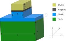
Schematic detail of a infinitesimal portion of the length of the waveguide used as a plasmonic sensor.
To reduce the size of the computational domain, PML of a rectangular type was employed. The PML simulates an infinite and non-reflective open domain by perfectly absorbing waves and preventing unwanted reflections within the computational domain under analysis. To avoid direct contact between the PML and the materials constituting the waveguide, they were positioned at a small distance over a region filled with air, in which the structure is immersed. The simulations considered that the dimensions on the PML exceeded the limits of the structure by 10% in all directions.
The simulations were performed using a original mathematical formulation [21] derived from the Helmholtz’s wave equation, obtained from Maxwell’s equations. The PML are introduced in the wave equation through a ∇ operator in Cartesian coordinates. After some mathematical considerations, a global matrix equation is obtained: [A](ϕ) = neff[B](ϕ), where [A] and [B] are matrices of complex and sparse nature. Moreover, this equation can be solved by using an iterative subspace method, where the refractive indices are directly incorporated into the calculations, with a computational window of 8 µm in the x axis and 8 µm in the y axis, discretizing in approximately 40.000 triangular elements [22]. Additionally, it was necessary to characterize the materials used based on their refractive indexes. The composition of the materials employed in this study is presented in Table I.
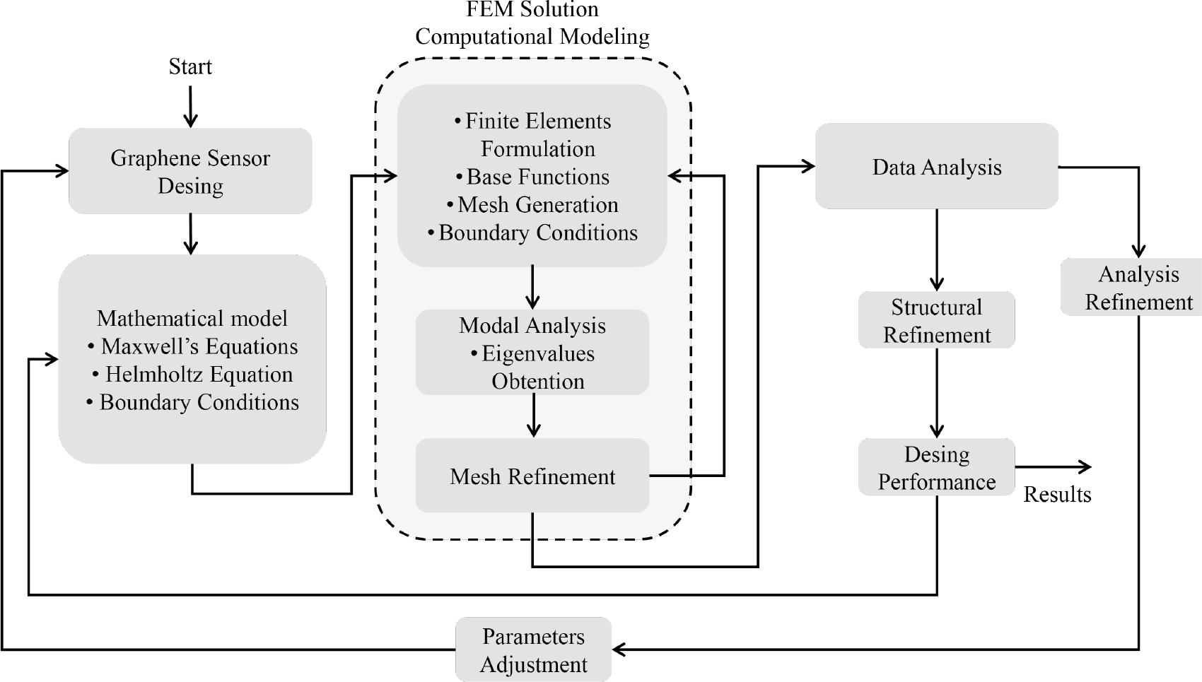
For the development of the graphene sensor project, it becomes necessary to validate the field confinement on the guiding region using computational modeling, Fig. 2 shows how the results were obtained using those simple steps in the algorithm.

Integral flowchart of the methodological process, simulation and methods utilized in this work.
The first step in the simulations involves designing the structure, considering all materials and boundaries that define each dimension to satisfy the design’s purpose. Next, a mesh is generated, discretizing each region into linear triangular elements for the Finite Elements method (FEM) with adaptive sizes, proportional to each region of the structure. The data are then introduced into a computational program [22] that uses the boundaries and materials of each region as inputs. This software produces a matrix of local node coordinates and a global node topology, associating each element with the corresponding material. In the subsequent step, the mesh information is processed by a computational program that performs the modal analysis of the structure, obtaining eigenvalues, which are related to the refractive indices of the materials present. After these procedures, the data analysis is performed. Adjustments are made to data processing and the performance is verified, if inconsistencies are found, adjustments are made to the structure.
The classical plasmonic model, in which is described the dielectric function of a free electron gas, was applied to determine the dielectric characteristics of the graphene sheet. From this modeling, the Drude-Lorentz model was applied to determine the dielectric characteristics of various materials and also establish a correlation between the dielectric functions of the plasmonic model. Thus, using this model, it is possible to determine the permittivity and dynamic conductivity of the graphene layers in optical frequencies. Equation 1 and Equation 2 shows the simplified version of Kubo’s formalism using a Drude-like intraband model for the dynamic conductivity and the permitivitty as a function of σ [35].
Where kb is the Boltzmann constant, τ is the scattering time, T is the temperature, Ef is the Fermi energy which can be approximated in for a Fermi speed of 106 m/s [35]. Equation 1 gives the intraband portion of the dynamic conductivity, which configures the largest contribution in terahertz conductivity, ωτ ≪ 1 [35], and the second term is the imaginary part of σs that is attributed to the interband conductivity, which is not shown in Equation 1, η is noted as the reduced Plank constant (). For high frequencies, where ωτ ≫ 1, in this way, Equation 2 provides the electrical permittivity ϵ = ϵrϵ0 as a function of the conductivity σs as shown in Equation 2 [34]. When light interacts with the interface, the surface plasmons appear in the surface region and can be described by a propagation constant of that plasmon wave. This propagation constant is well defined and continuous along the interface and can be defined in Equation 3 [36].
Where ϵm is the relative permittivity of the conductive material and ϵd is the relative permittivity of the dielectric materials.
Using this theory in the algorithm described in Fig. 2, it was possible to determine the dielectric characteristics of the graphene sheet and initiate the full analysis.
The first parameter analyzed was the electric field (E-field) at the graphene-dielectric interface, where surface plasmons (SP) occur. Therefore, the analysis of the electric field was carried out, mainly, on the graphene. This analysis was conducted on the structure in one-dimensional and two-dimensional form to evaluate the performance of the sensor in different DMSO concentrations used as a sample. Another parameter used to measure the sensor performance was the confinement losses (CL). These losses indicate the dissipation of optical energy in the confinement regions, due to the non-uniform geometry of the material. This parameter can be determined according to Equation 4 [15], [18]. The CL is an important parameter for analyzing the sensor performance, as it represents a critical factor in the performance of the proposed device, providing a measure of light confinement within the guiding region.
Where neff is the effective refractive index and λ is the wavelength in micrometers.
Next, the sensor sensitivity was evaluated from two main perspectives: spectral sensitivity and amplitude sensitivity. Spectral sensitivity was determined by analyzing the shift in the resonance wavelength in response to changes in the refractive index of the sensing medium, allowing for the quantification of the sensor ability to detect small variations in the environment. Spectral sensitivity, also referred to as wavelength sensitivity (WS), in nm per refractive index unit (RIU), was determined according to Equation 5 [15], [18], for λ given in nanometers.
Different from WS, the amplitude sensitivity (AS) measures how small are the changes in the refractive index, induced by molecular interactions or other chemical alterations, result in detectable variations in the intensity of the reflected light. That way, the higher the amplitude sensitivity, the more effective the sensor is at detect variations in concentration of the samples. This characteristic is extremely important for applications in biosensors, where it is important to detect low concentrations of substances. The amplitude sensitivity was determined using Equation 6 [37], [38].
Where CL(na,λ) represents the confinement losses, ∂CL(na,λ) is the difference between adjacent confinement losses, and ∂na is the difference between the adjacent refractive index of each sample.
Finally, to evaluate the overall efficiency of the plasmonic sensor, the Fig. of merit (FOM) was calculated. The FOM takes into account both spectral sensitivity and the linewidth of the plasmonic resonance, allowing for a more comprehensive assessment of the sensor performance. A high FOM indicates that the sensor is not only sensitive but also has a well-defined resonance, which is important for accuracy in detecting changes in the refractive index. Equation 7 [36], [37] was used to determine this parameter as shown in Equation 4.
WS denotes spectral sensitivity and FWHM represents the full width at half maximum of the plasmonic resonance, which indicates the wavelength range around the resonance peak where the intensity decreases to 50% of its peak value.
Thus, the methodological process followed this logical sequence, integrating modeling, data analysis, and efficiency assessment to ensure the robustness and accuracy of the developed plasmonic sensor.
III. RESULTS
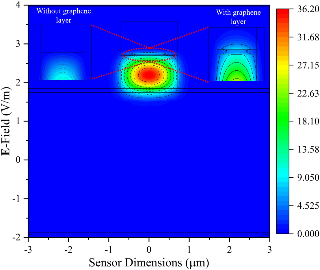
The first analysis performed on the device was modal analysis. This involved examining the E-field distributions. Due to the geometry of the proposed sensor, it was observed that surface plasmons appear only for the y-polarized mode, thus, all analyses were based on this polarization. Fig. 3 illustrates the E-field distribution for the case where the excitation wavelength is λ = 0.6329 µm and the DMSO concentration is 50%.
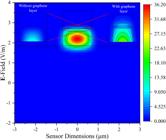
Two-dimensional E-field, in the rib waveguide cross-section, for λ =0.6329 µm and DMSO concentration at 50%.
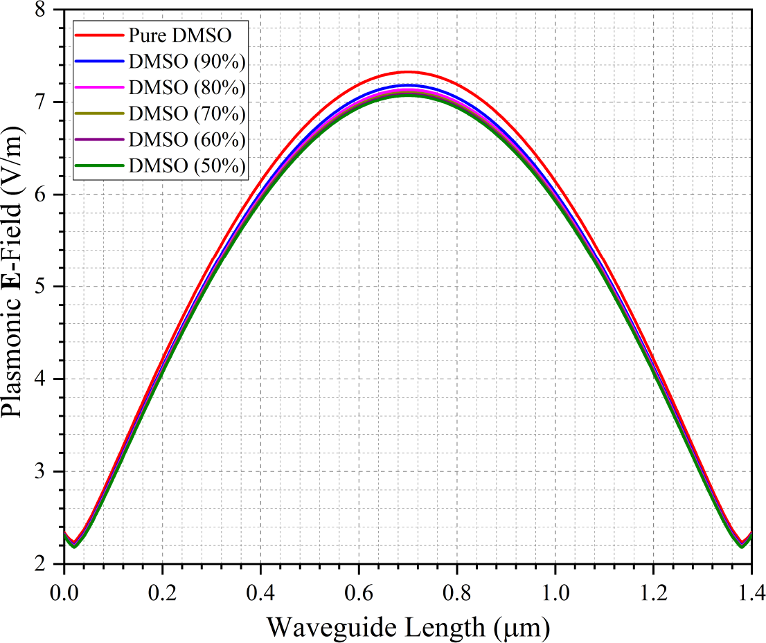
Figure 3 has special emphasis on the plasmonic effects at the graphene interface between the waveguide region and the DMSO analyte. The region where the plasmonic effect occurs is highlighted with a dashed red line. On the upper right side highlights the interface with a graphene multilayer placed between the waveguide guiding region and the DMSO analyte. On the upper left side the same interface is highlighted without the graphene multilayer between the waveguide guiding region and the DMSO analyte. It is observed that, when the graphene multilayer is removed, the surface plasmon resonance phenomenon is absent, making it impossible to use the structure as a plasmonic sensor. Hence, the interaction of this signal with the graphene layer induces the emergence of surface plasmons in the sample region, with a specific intensity. Fig. 3 also shows that the PML used are absorbing any incident waves, as no significant signals are observable in their adjacent regions. To detail and simplify the E-field analysis, it is more convenient to examine the distributions in a onedimensional manner. Additionally, this approach allows for a focused study of the plasmonic mode, which is the most relevant for sensing applications. In this context, Fig. 4 presents the plasmonic mode for various DMSO concentrations used.
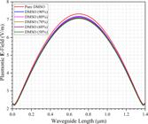
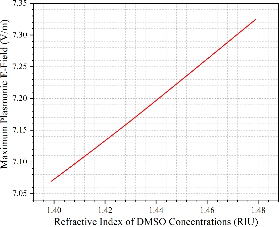
It is observable that the intensity of the plasmonic mode increased and the intensity of the fundamental mode decreased. This phenomenon was anticipated as it involves an energy exchange due to coupling between the modes. Even with the slight variations in plasmonic fields observed for the DMSO variant analyzed, the sensor is expected to demonstrate high sensitivity and efficiency. It was also evident that, as the concentrations of DMSO increased, the intensity of the plasmonic mode increased in a nearly linear manner, as illustrated in Fig. 5.
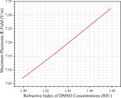
The result shown significant promise as it provides an initial parameter to evaluate the sensor’s interaction with different DMSO concentrations. Based on the E-field maximum value, it is possible to determine the concentration being applied to the sensor. Additionally, the near linearity of the response is important, as it makes the interpolation of data more accurate and reduces the error in extrapolation.
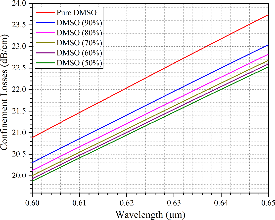
The next analysis performed was on the confinement losses. The device was designed to operate at a wavelength of λ = 0.6329 µm. However, in the simulations, a wavelength range from 0.60 µm to 0.65 µm was applied to represent the behavior of confinement losses across this range, as presented in Fig. 6.
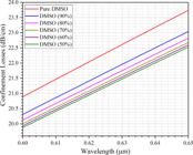
The confinement losses maintain stable responses across the investigated wavelength range. Additionally, it becomes evident that as the DMSO doping level increases, there is a corresponding rise in the confinement losses. This characteristic is particularly advantageous for plasmonic sensibility, as it allows for a clear differentiation of the material under test based on the observed variations in confinement losses.
Complementing Fig. 6, Table II presents the specific confinement loss values at the design wavelength of λ = 0.6329 µm. These values provide a precise assessment of the losses when the sensor is excited at this wavelength, offering detailed insight into the sensor’s performance under these conditions.
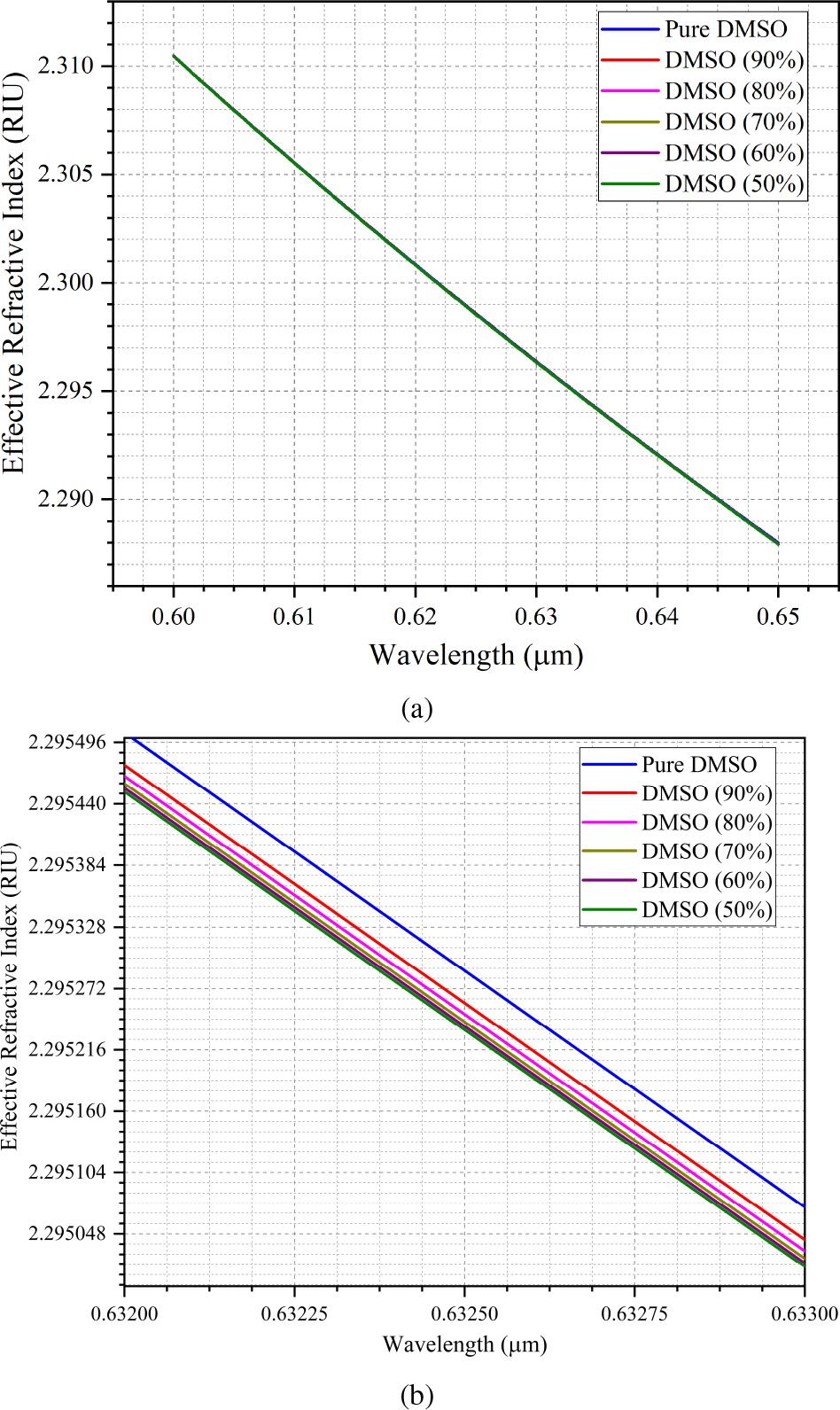
Following the flowchart, the spectral sensitivity of the proposed sensor will be analyzed next. However, a preliminary analysis of the effective refractive index as a function of the wavelength is necessary. Fig. 7 illustrates the behavior of the effective refractive index for various concentrations of DMSO.
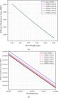
Effective refractive index of proposed sensor for various DMSO concentrations where (a) ranges from a gap of 0.05 µm and (b) provides a detailed view around the wavelength proposed for the design of 0.6329 µm
It is observable in the curves that the effective refractive index curves exhibit negligible variations for the different DMSO concentrations used. Additionally, within the adopted wavelength range, the variation in refractive index was approximately 0.022 RIU. These characteristics are important as they suggest a high average sensitivity.
Subsequently, the results for spectral and amplitude sensitivities will be presented. However, sensitivity calculations only provide point values, which makes the use of an interpolation method necessary to demonstrate the results through graphs. Initially, the Ordinary Least Squares (OLS) method was employed, however, the resulting polynomial order was excessively high, and the error was not minimized sufficiently. Following OLS, Newton [38] and Lagrange [39] interpolation methods were applied, but both presented errors that rendered the response analysis unfeasible, such as high ripples due to the Runge phenomenon.
Therefore, to address these problems, a code was implemented that performed data interpolation using cubic splines [40]. A cubic spline is a piecewise-defined function, with its structure composed of cubic polynomials between adjacent points. By dividing the domain into adjacent points, each segment between the points (xi,yi) and (xi+1,yi+1) is expressed according to Equation 8.
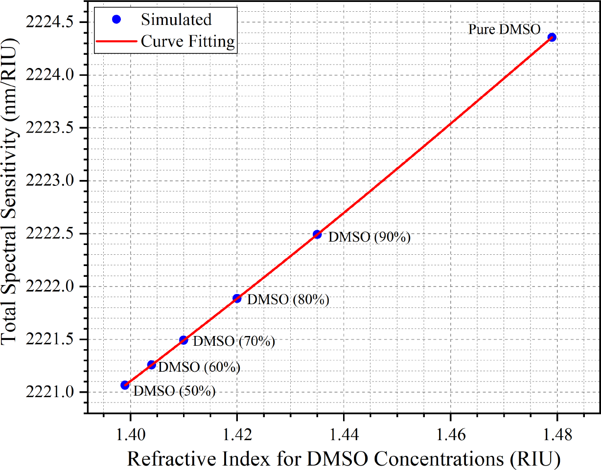
The study of spectral sensitivity was performed in three stages, where the total sensitivity, average sensitivity, and local sensitivity at λ = 0.6329 µm were calculated. Fig. 8 presents the total spectral sensitivity, which refers to the overall variation in the resonance wavelength across the entire measurement range, providing an initial view of how the sensor responds to changes in the refractive index over a broad spectral range. Fig. 8 shows the behavior of spectral sensitivity over the incremental increase of DMSO concentrations.
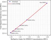
Refractive index of the proposed rib waveguide sensor for various DMSO concentrations versus total spectral sensitivity (nm/RIU).
The total sensitivity is observed to be approximately 2222 nm/RIU, with the highest sensitivity occurring for the pure DMSO sample (2224.37 nm/RIU) and the lowest sensitivity for the 50% DMSO concentration sample (2221.07nm/RIU).
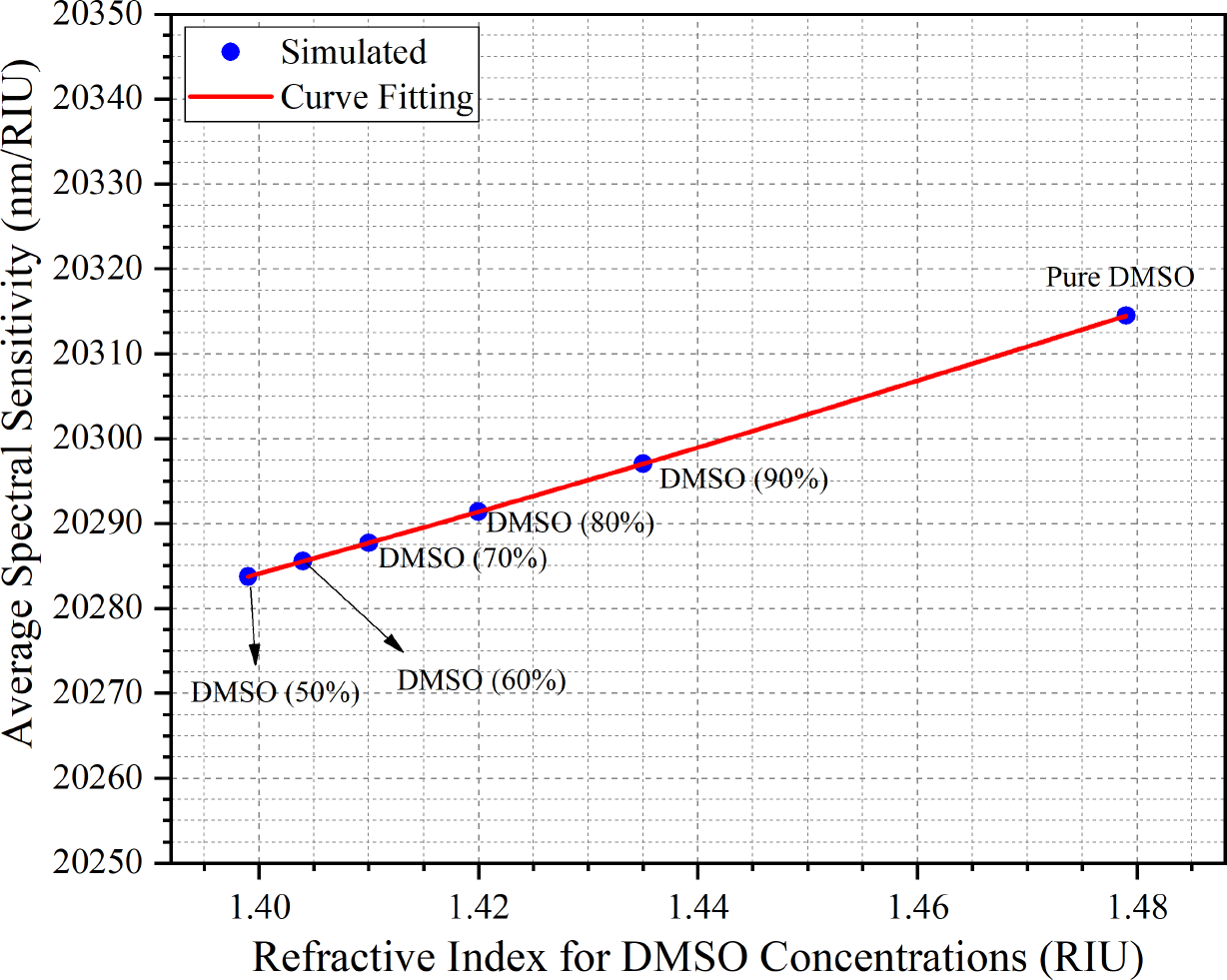
To complement this result, Fig. 9 shows the curves of average spectral sensitivity, which represents the average sensitivity calculated over specific wavelength intervals, offering a measurement of the sensor’s response in a central region of the spectrum.
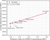
Refractive index of the proposed rib waveguide sensor for various DMSO concentrations versus average spectral sensitivity (nm/RIU)
Similarly to Fig. 8, the curves of refractive index demonstrates that the average sensitivity is higher for greater concentrations of DMSO. However, it is noticeable that the sensitivities obtained are significantly higher. This is caused by, in the case of average sensitivity, how the calculations are performed over a specific, and generally smaller wavelength interval, allowing for a more precise analysis of the sensor in a particular region.
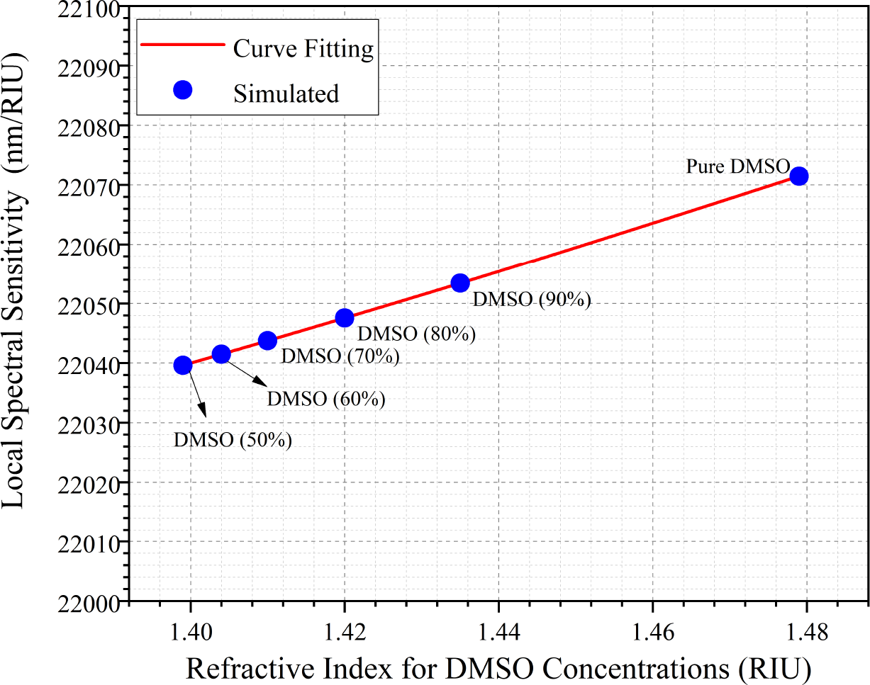
In this context, by analyzing an extremely narrow range, it is possible to obtain the concept of local spectral sensitivity, which focuses on the variation of the resonance wavelength at a specific point or within a narrow range, providing a detailed analysis of the sensor’s response to changes in the refractive index in a very specific spectral region. In addition, Fig. 10 presents the local spectral sensitivity curve for the excitation wavelength of λ = 0.6329 µm.
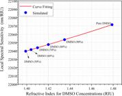
Local Spectrum Sensitivity in nm/RIU for a range of Refractive Index for DMSO Concentrations.
The response shows that, for the excitation wavelength, the spectral sensitivity is increased, but remained around values close to 22,000 nm/RIU. Additionally, the curve exhibits a increasing behavior, corroborating the results presented in Fig. 8 and 9. The local analysis of spectral sensitivity becomes necessary as it clearly demonstrates the sensor’s capability when excited at the excitation wavelength. Table III provides a summary of the spectral sensitivity analysis in its total, average, and local forms shown by Fig. 8, 9 and 10.
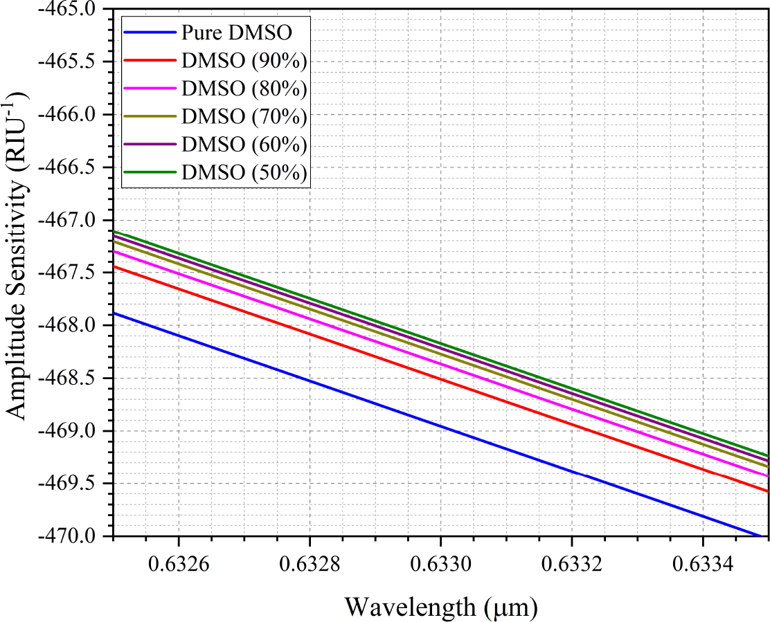
Following the analysis of spectral sensitivity, Fig. 10 presents the amplitude sensitivity curves when the sensor is excited at its design wavelength of λ = 0.6329 µm. Fig. 11 illustrates the amplitude sensitivity curve across the entire wavelength range, extending from 0.6 µm to 0.65 µm.
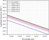
Provided a zoomed-in view for values close to the design wavelength, it is possible to observe that the peak values of AS are higher for greater concentrations of DMSO. The data for the relevant specific values obtained for the design wavelength are shown in Table IV.
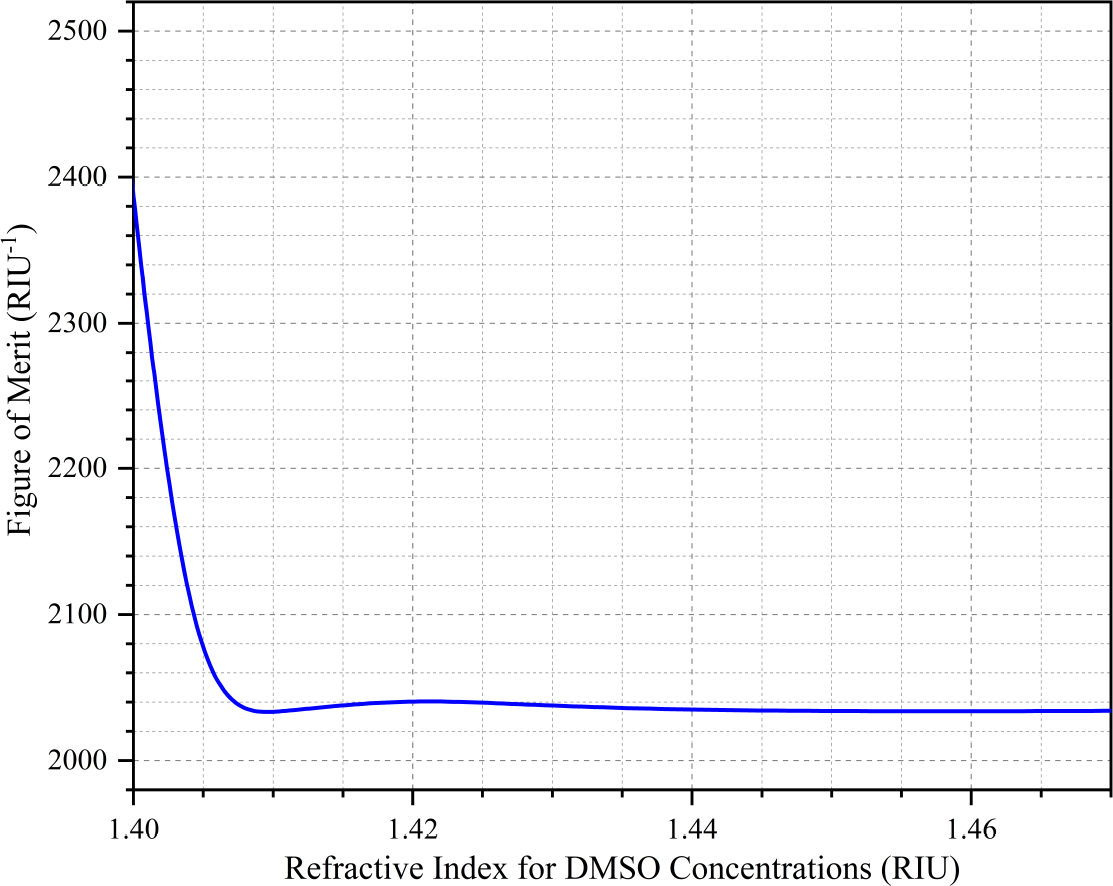
Ending the methodological process for data analysis, Fig. 12 presents the Figure of Merit (FOM) for the proposed sensor, representing the ratio of spectral sensitivity of the half-power plasmonic field.
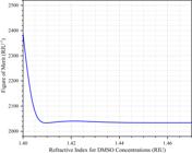
Figure of Merit (RIU-1) for a range of Refractive Index of different DMSO Concentrations (RIU).
The FOM for the design is approximately 2050 RIU-1 for the tested DMSO concentrations, except for the 50% DMSO concentration, which yielded an FOM of 2478 RIU-1. These values are relatively high, indicating a generally good performance of the sensor for the tested DMSO concentrations. The higher FOM at the 50% DMSO concentration suggests that the sensor is more precise when detecting this sample, though less sensitive, as demonstrated throughout the results. This is attributed to a more effective optical interaction or an optimized resonance configuration for this specific concentration. To better contextualize this work, other studies in the literature, as shown in Table V, were considered in order to compare the parameters analyzed in this article.
Gathered all resources from simulations it becomes necessary to compile the information and evaluate the sensor’s performance in comparison to those cited in recent literature and in sequence evaluate it’s effectiveness as a sensor in He-Ne laser-beam systems for the current application.
IV. CONCLUSIONS
In conclusion, results shown that the application of graphene as a plasmonic material in the development of a new plasmonic sensor model, designed to operate in the red region, is a viable solution. The developed sensor was based on optical principles and can be used as a biosensor, when adjusting the concentration levels of DMSO in analyte samples, and graphene proves to be a viable solution due to its facilitation of the LSPR effect, which becomes sensitive to variations in the refractive index of DMSO at tunable optical frequencies. To enhance the sensor’s functionality a rib waveguide was utilized, consisting of a dielectric substrate composed of Ta2O5 and a top layer with a ridge made of Nb2O5, forming the guiding region. The sensor model utilizes graphene to excite surface plasmons, making the fabrication of the structure more cost-effective compared to sensors that use noble metals, such as gold or platinum, to achieve the similar effect. By employing a rib waveguide, the device has the potential to be developed into miniaturized systems, as its manufacturing can be accomplished using lithographic techniques. Numerical results demonstrated that the proposed device efficiently detects DMSO concentrations with refractive indices ranging from 1.399 to 1.479. The sensor achieved a local spectral sensitivity of approximately 22,000 nm/RIU for all DMSO concentrations, and the amplitude sensitivity values were also satisfactory. Finally, with a Figure of Merit (FOM) exceeding 2000, the sensor has demonstrated exceptional efficiency and reliability in identify varying levels of DMSO concentrations. When compared to the experimental results in the literature this present report show satisfying results as shown in Table V, which enforces the excellent performance of the proposed sensor.
ACKNOWLEDGMENTS
The authors would like to thank the Federal University of Rio Grande do Norte, Electrical and Computer Engineering Graduate Program and Federal University of Semiarid Region for support and encouragement in the production of this work. This article was financed in part by the Coordenação de Aperfeiçoamento de Pessoal de Nível Superior - Brasil (CAPES) - Financing Code 001. This present study was realized with the support of CNPq, Conselho Nacional de Desenvolvimento Científico e Tecnológico - Brasil (Proc. 140380/2022-1).
REFERENCES
- [1] B. Ahluwalia, I. Helle, and O. Helles, “Rib waveguides for trapping and transport of particles,” Optics Express, vol. 24, pp. 4477-4487, 2016.
- [2] R. Brandel and D. Bormann, “An infrared dielectric function model for amorphous solids,” Journal of Applied Physics, vol. 71, pp. 1-6, 1992.
- [3] M. C. Gwinner, S. Khodabakhsh, M. H. Song, H. Schweizer, H. Giessen, and H. Sirringhaus, “Integration of a rib waveguide distributed feedback structure into a light-emitting polymer field-effect transistor,” Advanced Functional Materials, vol. 19, p. 1360-1370, 2009.
- [4] H. Zhang, G. Fan, S. Li, X. Cai, J. Wei, and G. Jing, “Integrated opto-mechanical cantilever sensor with a rib waveguide,” Microscopy (Oxford, U. K.), vol. 286, pp. 240-244, 2022.
- [5] N. Shrikant, C. T. Chandrika, J. Raviprasad, T. Srinivas, and G. Prashanth, “Design and analysis of rib waveguide bragg grating for multiplexed biosensing application,” in Proceedings of the 2021 IEEE International Conference on Electronics, Computing and Communication Technologies (CONECCT), pp. 1-5, 2021.
- [6] V. Lavchiev, R. Holly, G. Chen, F. Shäffler, R. Goldhahn, and W. Jantsch, “Si rib waveguide photodetector with an ordered array of ge islands for 1.5 µm,” Optics Letters, vol. 34, pp. 3785-3787, 2009.
- [7] M. A. Mahdian, M. Nikoufard, and F. Soleimannezhad, “Effect of etching depth on the performance of inp-based hybrid plasmonic waveguides,” International Journal Of Electronics and Communication, vol. 126, pp. 153403-153411, 2020.
- [8] D. Kong et al., “Sp2-carbon dominant carbonaceous materials for energy conversion and storage,” Materials Science and Engineering: R: Reports, vol. 137, pp. 1-37, 2019.
- [9] A. J. Samuels and J. D. Carey, “Engineering graphene conductivity for flexible and high-frequency applications,” ACS Applied Materials Interfaces, vol. 7, pp. 22246-22255, 2015.
- [10] C. Tang et al., “Narrow-band absorption enhancement and modulation of single layer graphene by surface plasmon polaritons in near-infrared region,” Phys. B: Condensed Matter, vol. 695, pp. 416521-416526-, 2024.
- [11] K. R. Paton et al., “Scalable production of large quantities of defect-free few-layer graphene by shear exfoliation in liquids,” Nature Materials, vol. 13, pp. 624-630, 2014.
- [12] J. Liu, S. Wang, Y. Wang, L. Zhu, and J. Liu, “A transmission grating-based polarization demodulated grating interferometric sensor,” in 2022 14th International Conference on Measuring Technology and Mechatronics Automation (ICMTMA), pp. 6-9, 2022.
- [13] S. Ogawa, S. Fukushima, and M. Shimatani, “Graphene plasmonics in sensor applications: A review,” Sensors, vol. 20, pp. 3563-3584, 2020.
- [14] T. Tene et al., “Role of graphene in surface plasmon resonance-based biosensors,” Sensors, vol. 24, pp. 4670-4710, 2024.
- [15] M. M. de Araújo and J. P. da Silva, “The design of glicerol concentration sensor based on an lrspp hybrid photonic biosensor,” Sensors, vol. 23, pp. 2010-2027, 2023.
- [16] Z. B. Zheng et al., “Tailoring of electromagnetic field localizations by two-dimensional graphene nanostructures,” Light: Science & Applications, vol. 6, pp. 17057-17065, 2017.
- [17] G. Melvin and K. Senthilnathan, “High sensitive d-shaped photonic crystal fiber sensor with v-groove analyte channel,” Optik, vol. 213, pp. 164779-164789, 2020.
- [18] N. H. O. Cunha and J. P. da Silva, “High sensitivity surface plasmon resonance sensor based on a ge-doped defect and d-shaped microstructured optical fiber,” Sensors, vol. 22, pp. 3220-3237, 2022.
- [19] V. Agieienko, V. Neklyudov, and A. Dimiev, “Solvent-induced changes in the graphene oxide absorption spectrum. the case of dimethylsulfoxide/water mixtures,” Journal of Molecular Liquids, vol. 287, pp. 110942-110950, 2019.
- [20] S. W. Jacob and D. C. Wood, “Dimethyl sulfoxide (dmso) toxicology, pharmacology, and clinical experience,” Americal Journal of Surgery, vol. 114, pp. 414-426, 1967.
- [21] D. Belhadj, A. Negadi, P. Venkatesu, I. Bahadur, and L. Negadi, “Density, speed of sound, refractive index and related derived/excess properties of binary mixtures (furfural+ dimethyl sulfoxide),(furfural+ acetonitrile) and (furfural+ sulfolane) at different temperatures,” Journal of Molecular Liquids, vol. 330, pp. 115436-115452, 2021.
- [22] J. P. da Silva, H. E. Hernández-Figueroa, and A. M. F. Frasson, “Improved vectorial finite-element bpm analysis for transverse anisotropic media,” Journal of Lightwave Technology, vol. 21, pp. 567-577, 2003.
- [23] J. P. da Silva, D. S. Bezerra, V. F. Rodriguez-Esquerre, I. E. da Fonseca, and H. E. Hernandez-Figueroa, “Ge-doped defect-core microstructured fiber design by genetic algorithm for residual dispersion compensation,” IEEE Photonics Technology Letters, vol. 22, pp. 1337-1339, 2010.
- [24] W. Du, L. Miller, and F. Zhao, “Numerical study of graphene/au/sic waveguide-based surface plasmon resonance sensor,” Biosensors, vol. 11, no. 11, pp. 455-463, 2021.
- [25] A. S. Almeida et al., “A critical analysis on the sensitivity enhancement of surface plasmon resonance sensors with graphene,” Nanomaterials, vol. 12, no. 15, p. 2562, 2022.
- [26] M. Cermak, N. Perez., M. Collins, and M. Baharami, “Material properties and structure of natural graphite sheet,” Scientific Reports, vol. 10, no. 18672, pp. 1-12, 2020.
- [27] W. Xu and others., “Surface enhanced raman spectroscopy on a flat graphene surface,” Proceedings of the National Academy of Sciences, vol. 109, no. 24, pp. 9281-9286, 2012.
- [28] J. Peña-Bahamonde, H. Nguyen, S. Fanourakis, and D. Rodrigues, “Recent advances in graphene-based biosensor technology with application in life sciences,” Journal of nanobiotechnology, vol. 16, pp. 75-92, 2018.
- [29] B. Janegitz and others., “The application of graphene for in vitro and in vivo electrochemical biosensing,” Biosensors and Bioelectronics, vol. 15, pp. 224-233, 2017.
- [30] L. Tony and P. Avouris, “Graphene plasmonics for terahertz to mid-infrared applications,” ACS Nano, vol. 8, pp. 1086- 1101, 2014.
- [31] F. Mezzapesa and others., “Terahertz frequency combs exploiting an on-chip, solution-processed, graphene-quantum cascade laser coupled-cavity,” ACS Photonics, vol. 7, pp. 3489-3498, 2020.
- [32] L. Gao, F. Lemarchand, and M. Lequime, “Exploitation of multiple incidences spectrometric measurements for thin film reverse engineering,” Optics Express, vol. 20, pp. 15734-15751, 2012.
- [33] B. Horcholle et al., “Growth and study of tb3+ doped nb2o5 thin films by radiofrequency magnetron sputtering: photoluminescence properties,” Applied Surface Science, vol. 597, pp. 153711-153728, 2022.
- [34] J. Weber, V. Calado, and M. van de Sanden, “Optical constants of graphene measured by spectroscopic ellipsometry,” Applied Physics Letters, vol. 97, pp. 091904-091908, 2010.
- [35] S. Abadal et al., “Graphene-based terahertz antennas for area-constrained applications,” in 2017 40th International Conference on Telecommunications and Signal Processing (TSP), pp. 817-820, 2017.
- [36] N. Luan, L. Zhao, Y. Lian, and S. Lou, “A high refractive index plasmonic sensor based on d-shaped photonic crystal fiber with laterally accessible hollow-core,” IEEE Photonics Journal, vol. 10, pp. 1-7, 2018.
- [37] M. Mollah and M. Islam, “Novel single hole exposed suspended core localized surface plasmon resonance sensor,” IEEE Sensors Journal, vol. 21, pp. 2813-2820, 2020.
- [38] F. Haslinger, “On newton’s interpolation polynomials,” Journal of Approximation Theory, vol. 22, pp. 352-355, 1978.
- [39] R. Al-Jarrah, “On the lagrange interpolation polynomials of entire functions,” Journal of Approximation Theory, vol. 41, pp. 170-178, 1984.
- [40] M. Marsden, “Cubic spline interpolation of continuous functions,” Journal of Approximation Theory, vol. 10, pp. 103- 111, 1974.
- [41] A. Yasli and H. Ademgil, “Geometrical comparison of photonic crystal fiber-based surface plasmon resonance sensors,” Optical Engineering, vol. 57, pp. 030801-030801, 2018.
- [42] Y. Monfared, M. Hajati, C. Liang, S. Yang, and M. Qasymeh, “Quasi-d-shaped fiber optic plasmonic biosensor for high-index analyte detection,” IEEE Sensors Journal, vol. 21, pp. 17-23, 2021.
- [43] M. Mahfuz, M. Hossain, E. Haque, N. Hai, Y. Namihira, and F. Ahmed, “Dual-core photonic crystal fiber-based plasmonic ri sensor in the visible to near-ir operating band,” IEEE Sensors Journal, vol. 20, pp. 7692-7700, 2020.
- [44] Z. Fan, S. Li, Q. Liu, G. An, H. Chen, J. Li, D. Chao, H. Li, J. Zi, and W. Tian, “High-sensitivity of refractive index sensor based on analyte-filled photonic crystal fiber with surface plasmon resonance,” IEEE Photonics Journal, vol. 7, pp. 1-9, 2015.
- [45] F. Haider, R. Aoni, R. Ahmed, M. Islam, and E. Miroshnichenko, “Propagation controlled photonic crystal fiber based plasmonic sensor via scaled-down approach,” IEEE Sensors Journal, vol. 19, pp. 962-969, 2019.
- [46] C. Zhang et al., “U-bent fiber optic spr sensor based on graphene/agnps,” Sensors and Actuators B: Chemical, vol. 251, pp. 127-133, 2017.